Sony 757MX Service Manual - Page 23
Printed, Wiring, Boards, Schematic, Diagrams - cd changer cdx
 |
UPC - 027242597846
View all Sony 757MX manuals
Add to My Manuals
Save this manual to your list of manuals |
Page 23 highlights
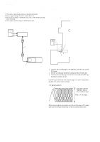
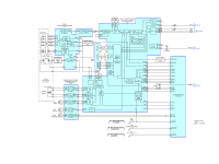
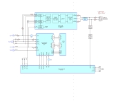
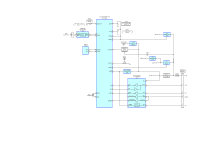
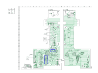
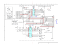
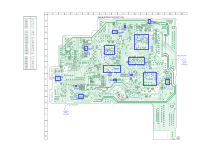
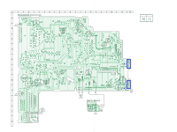
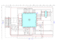
6-4. NOTE FOR PRINTED WIRING BOARDS AND SCHEMATIC DIAGRAMS Note on Printed Wiring Board: • X : parts extracted from the component side. • Y : parts extracted from the conductor side. • f : internal component. • : Pattern from the side which enables seeing. (The other layers' patterns are not indicated.) Caution: Pattern face side: (Conductor Side) Parts face side: (Component Side) Parts on the pattern face side seen from the pattern face are indicated. Parts on the parts face side seen from the parts face are indicated. Note on Schematic Diagram: • All capacitors are in µF unless otherwise noted. pF: µµF 50 WV or less are not indicated except for electrolytics and tantalums. • All resistors are in Ω and 1/4 W or less unless otherwise specified. • f : internal component. • C : panel designation. Note: The components identified by mark 0 or dotted line with mark 0 are critical for safety. Replace only with part number specified. Note: Les composants identifiés par une marque 0 sont critiques pour la sécurité. Ne les remplacer que par une pièce portant le numéro spécifié. • A : B+ Line. • H : adjustment for repair. • Power voltage is dc 14.4V and fed with regulated dc power supply from CD changer controller. • Voltages and waveforms are dc with respect to ground in CD play conditions. no mark : CD PLAY ∗ : Impossible to measure • Voltages are taken with a VOM (Input impedance 10 MΩ). Voltage variations may be noted due to normal production tolerances. • Waveforms are taken with a oscilloscope. Voltage variations may be noted due to normal production tolerances. • Circled numbers refer to waveforms. • Signal path. J : CD PLAY • Circuit Boards Location JACK board SWITCH board LSW board CDX-757MX MAIN board RF board 23 23
-
 1
1 -
2
-
3
-
4
-
5
-
6
-
7
-
8
-
9
-
10
-
11
-
12
-
13
-
14
-
15
-
16
-
17
-
 18
18 -
 19
19 -
 20
20 -
 21
21 -
 22
22 -
 23
23 -
 24
24 -
 25
25 -
 26
26 -
 27
27 -
 28
28 -
29
-
30
-
31
-
32
-
33
-
34
-
35
-
36
-
37
-
38
-
39
-
40
-
41
-
42
-
43
-
44
-
45
-
46
-
47
-
48
-
49
-
50
-
51
-
52
-
53
-
54
-
55
-
56
-
57
-
58
-
59
-
60
-
61
-
62
-
63
 |
 |
