Sony 757MX Service Manual - Page 40
Pin No., Pin Name, Description
 |
UPC - 027242597846
View all Sony 757MX manuals
Add to My Manuals
Save this manual to your list of manuals |
Page 40 highlights
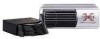
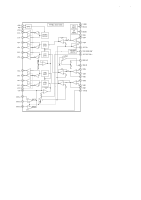
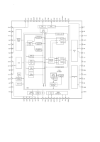
CDX-757MX Pin No. 54 55, 56 57 58 59 60 61 62 63 64 65 66 67 68 69 70, 71 72 73 74 75 76 77 78 79 80 81 82 83 84 85 86 to 89 90 91 92 93, 94 95 96 97 Pin Name AVCC MD0, MD1 OSC2 OSC1 RES NMI STBY VCC XTAL VSS EXTAL FEW MD2 FL BOOT FL W NC MGLK-SW DECINT NC EJECT SO SI SCLK EEDATA SDA SCL EECLK NC SQSO SQCK NC R/RW SEL BUSON BUCHK NC LOADF LOADR SINGLE 98 LOAD SW 99 SAVE SW 100 LIM SW I/O Description - Power supply terminal (+3.3V) (for A/D converter) I Setting terminal for the CPU operational mode "H": single chip mode (fixed at "H" in this set) O Sub system clock output terminal Not used I Sub system clock input terminal Not used (fixed at "L") I System reset signal input from the SONY bus interface and reset signal generator "L": reset For several hundreds msec. after the power supply rises, "L" is input, then it changes to "H" O Not used (fixed at "H") O Standby mode control signal output terminal Not used (fixed at "H") - Power supply terminal (+3.3V) I Main system clock input terminal (12.288 MHz) - Ground terminal O Main system clock output terminal (12.288 MHz) I Flash memory data write enable signal input terminal I Setting terminal for the CPU operational mode "H": single chip mode (fixed at "H" in this set) I Flash memory data write control signal input terminal "L" active O Flash memory data write control signal output (connecting FEW (pin 66)) O Not used I Magazine in/out detect switch input terminal "L": magazine in I Interrupt signal input from the CD-ROM/MP3 decoder O Not used I Eject switch input terminal "L" active O Serial data output to the SONY bus interface I Serial data input from the SONY bus interface I Serial data transfer clock signal input from the SONY bus interface I/O Two-way data bus with the EEPROM I/O I2C interface data input/output with the CD-ROM/MP3 decoder O I2C interface data transfer clock signal output to the CD-ROM/MP3 decoder O Serial data transfer clock signal output to the EEPROM O Not used I Subcode Q data input from the DSP O Subcode Q data reading clock signal output to the DSP O Not used O CD-ROM/RW selection signal output "L": CD-RW, "H": CD-ROM I Bus on/off control signal input from the SONY bus interface "L": bus on I Battery detection signal input "H": low battery (Normally: "L") O Not used O Motor drive signal (load chucking direction) output to the chucking motor drive O Motor drive signal (save direction) output to the chucking motor drive I Setting terminal for the single disc/multiple discs mode "L": single disc mode, "H": multiple discs mode (fixed at "H" in this set) I Chucking end detect switch input terminal "L": When completion of the disc chucking operation I Save end detect switch input terminal "L": When completion of the disc save operation I Sled limit in detect switch input terminal "L": When the optical pick-up is inner position 40
-
 1
1 -
2
-
3
-
4
-
5
-
6
-
7
-
8
-
9
-
10
-
11
-
12
-
13
-
14
-
15
-
16
-
17
-
18
-
19
-
20
-
21
-
22
-
23
-
24
-
25
-
26
-
27
-
28
-
29
-
30
-
31
-
32
-
33
-
34
-
 35
35 -
 36
36 -
 37
37 -
 38
38 -
 39
39 -
 40
40 -
 41
41 -
 42
42 -
 43
43 -
 44
44 -
 45
45 -
46
-
47
-
48
-
49
-
50
-
51
-
52
-
53
-
54
-
55
-
56
-
57
-
58
-
59
-
60
-
61
-
62
-
63
 |
 |