Sony HCD-DH7BT Service Manual - Page 66
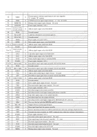
Pin No., Pin Name, Description
 |
View all Sony HCD-DH7BT manuals
Add to My Manuals
Save this manual to your list of manuals |
Page 66 highlights
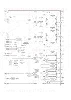
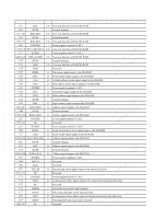
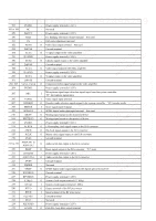
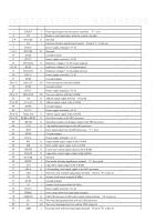
HCD-DH3/DH5BT/DH7BT http://www.xiaoyu163.com TEL 13942296513 QQ 376315150 892498299 TEL 13942296513 QQ 376315150 892498299 QQ 376315150 892498299 PinNo. PinName I/O Description 49 WIDE O Normal/squeeze selection signal output to the video amplifier "L": normal, "H": squeeze 50 MSW O CD/DVD selection signal output terminal "L": CD, "H": DVD 51 MAMUTE O Muting control signal output terminal Not used 52 DVDD18 - Power supply terminal (+1.8V) 53 to 61 IOA2 to IOA8, IOA18, IOA19 O Address signal output to the flash ROM 62 DVSS - Ground terminal 63 APLLCAP - Connection terminal for an external capacitor 64 APLLVSS - Ground terminal 65 VDD3 - Power supply terminal (+3.3V) 66 IOWR O Write enable signal output to the flash ROM 67 to 72 IOA16 to IOA11 O Address signal output to the flash ROM 73 DVDD3 - Power supply terminal (+3.3V) 74 to 76 IOA10, IOA9, IOA20 O Address signal output to the flash ROM 77 IOCS O Chip select signal output to the flash ROM 78 IOA1 O Address signal output to the flash ROM 79 IOOE O Output enable signal output to the flash ROM 80 DVDD3 - Power supply terminal (+3.3V) 81 to 84 AD0 to AD3 I/O Data/address signal input/output terminal with the flash ROM TEL 13942296513 QQ 376315150 892498299 85 86 to 88 DVSS AD4 to AD6 - Ground terminal I/O Data/address signal input/output terminal with the flash ROM 89 IOA21 O Address signal output to the flash ROM 90 ALE O Address latch enable signal output terminal Not used 91 AD7 I/O Data/address signal input/output terminal with the flash ROM 92, 93 IOA17, IOA0 O Address signal output to the flash ROM 94 DVSS - Ground terminal 95 UWR O Write enable signal output terminal Not used 96 URD O Data read enable signal output terminal Not used 97 DVDD18 - Power supply terminal (+1.8V) 98 IFSDO O Serial data output to the system controller 99 IFCK O Serial data transfer clock signal output to the system controller 100 XIFCS O Chip select signal output to the system controller 101 IFSDI I Serial data input from the system controller 102 SCL O Serial data transfer clock signal output to the EEPROM and D/A converter 103 SDA I/O Two-way data bus with the EEPROM and D/A converter 104 TRG-SW I Trigger detection switch input terminal 105 IFBSY I Busy signal input from the system controller 106 RXD I Receive data input terminal for UART communication when data writing to flash memory 107 TXD O Transmit data output terminal for UART communication when data writing to flash memory 108 DVDD3 - Power supply terminal (+3.3V) 109 ICE www . 110 PRST 111 IR 112 INT0 113 DQM0 I ICE mode enable signal input terminal Not used xiaoy u163. com I Reset signal input from the system controller "L": reset I IR control signal input terminal Not used O Interrupt request signal output terminal Not used O Data mask signal output to the SD-RAM 114 MREQ O Muting request signal output terminal Not used 66 http://www.xiaoyu163.com
-
 1
1 -
2
-
3
-
4
-
5
-
6
-
7
-
8
-
9
-
10
-
11
-
12
-
13
-
14
-
15
-
16
-
17
-
18
-
19
-
20
-
21
-
22
-
23
-
24
-
25
-
26
-
27
-
28
-
29
-
30
-
31
-
32
-
33
-
34
-
35
-
36
-
37
-
38
-
39
-
40
-
41
-
42
-
43
-
44
-
45
-
46
-
47
-
48
-
49
-
50
-
51
-
52
-
53
-
54
-
55
-
56
-
57
-
58
-
59
-
60
-
 61
61 -
 62
62 -
 63
63 -
 64
64 -
 65
65 -
 66
66 -
 67
67 -
 68
68 -
 69
69 -
 70
70 -
 71
71 -
72
-
73
-
74
-
75
-
76
-
77
-
78
-
79
-
80
-
81
-
82
-
83
-
84
-
85
-
86
-
87
-
88
-
89
-
90
-
91
-
92
-
93
-
94
-
95
-
96
-
97
-
98
-
99
-
100
-
101
-
102
-
103
-
104
-
105
-
106
-
107
-
108
-
109
-
110
-
111
-
112
-
113
-
114
-
115
-
116
-
117
-
118
-
119
-
120
-
121
-
122
-
123
-
124
-
125
-
126
-
127
-
128
-
129
-
130
 |
 |
