Sony HCD-DH7BT Service Manual - Page 76
O-sm Nsp Mute, I-key1 To I-key3 - hcd bluetooth pin
 |
View all Sony HCD-DH7BT manuals
Add to My Manuals
Save this manual to your list of manuals |
Page 76 highlights
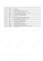
HCD-DH3/DH5BT/DH7BT http://www.xiaoyu163.com TEL 13942296513 QQ 376315150 892498299 TEL 13942296513 QQ 376315150 892498299 QQ 376315150 892498299 PinNo. PinName I/O Description 46 I-MTK CLK I Serial data transfer clock signal input from the servo DSP 47 AVREF1 I Reference voltage (+3.3V) input terminal (for D/A converter) 48 O-SM NSP MUTE O NSP muting control signal output to the stream processor 49 O-SM INIT O Initialize signal output to the stream processor 50 AVREF0 I Reference voltage (+3.3V) input terminal (for A/D converter) 51 AVSS - Ground terminal 52 to 55 I-SPEC1 to I-SPEC4 I Setting terminal for the destination 56 to 58 I-KEY1 to I-KEY3 I Top and front panel key input terminal (A/D input) 59 I-AC DET I AC power detection signal input terminal 60 O-USB SO O Ready to send signal output to the USB controller (DH3/DH5BT) 61 I-USB SI I Clear to send signal input from the USB controller (DH3/DH5BT) 62 to 64 NC O Not used 65 O-BT AV ROL O Transmission/reception mode notification signal output to the bluetooth module (DH5BT/DH7BT) 66 I-BT CTS I Clear to send signal input from the bluetooth module (DH5BT/DH7BT) 67 O-BT RTS O Ready to send signal output to the bluetooth module (DH5BT/DH7BT) 68 O-BT REST O Reset signal output to the bluetooth module "L": reset (DH5BT/DH7BT) 69 NC O Not used 70 O-SBY LED O LED drive signal output terminal for STANDBY indicator "L": LED on 71 I-BT RXD I Serial data input from the bluetooth module (DH5BT/DH7BT) 72 O-BT TXD O Serial data output to the bluetooth module (DH5BT/DH7BT) TEL 13942296513 QQ 376315150 892498299 73 O-FL RST O Reset signal output to the fluorescent indicator tube driver "L": reset 74 O-FL CE O Chip enable signal output to the fluorescent indicator tube driver 75 O-POWER O Sub power on/off control signal output terminal "H": power on 76 O-XM TXD/ O-USB TXD O Serial data output to the USB controller (DH3/DH5BT) Serial data output to the XM receiver (DH7BT) 77 I-XM RXD/ I-USB RXD I Serial data input from the USB controller (DH3/DH5BT) Serial data input from the XM receiver (DH7BT) 78 NC O Not used 79 I-USB RXD I Serial data input from the USB controller (DH3/DH5BT) 80 I-BT RXD I Serial data input from the bluetooth module (DH5BT/DH7BT) 81 I-RMC I SIRCS signal input from the remote control receiver 82 NC O Not used 83 I-WAKE UP I Wake up signal input terminal 84 O-FL DATA O Serial data output to the fluorescent indicator tube driver 85 O-ST CE O Chip enable signal output to the tuner (FM/AM) 86 O-FL CLK O Shift clock signal output to the fluorescent indicator tube driver 87 O-ST DATA O Serial data output to the tuner (FM/AM) 88 O-ST CLK O Serial data transfer clock signal output to the tuner (FM/AM) 89 TOOL0 I Writing terminal 90 RESET I System reset signal input from the reset signal generator "L": reset For several hundreds msec. after the power supply rises, "L" is input, then it changes to "H" 91 XT2 O Sub system clock output terminal (32.768 kHz) www 92 XT1 93 FLMD0 94 95 . X2 X1 I Sub system clock input terminal (32.768 kHz) xiaoy u163. I Flash memory programming mode setting terminal O Main system clock output terminal (20 MHz) I Main system clock input terminal (20 MHz) com 96 REGC - External capacitor connection terminal for regulator output of internal operation 76 http://www.xiaoyu163.com
-
 1
1 -
2
-
3
-
4
-
5
-
6
-
7
-
8
-
9
-
10
-
11
-
12
-
13
-
14
-
15
-
16
-
17
-
18
-
19
-
20
-
21
-
22
-
23
-
24
-
25
-
26
-
27
-
28
-
29
-
30
-
31
-
32
-
33
-
34
-
35
-
36
-
37
-
38
-
39
-
40
-
41
-
42
-
43
-
44
-
45
-
46
-
47
-
48
-
49
-
50
-
51
-
52
-
53
-
54
-
55
-
56
-
57
-
58
-
59
-
60
-
61
-
62
-
63
-
64
-
65
-
66
-
67
-
68
-
69
-
70
-
 71
71 -
 72
72 -
 73
73 -
 74
74 -
 75
75 -
 76
76 -
 77
77 -
 78
78 -
 79
79 -
 80
80 -
 81
81 -
82
-
83
-
84
-
85
-
86
-
87
-
88
-
89
-
90
-
91
-
92
-
93
-
94
-
95
-
96
-
97
-
98
-
99
-
100
-
101
-
102
-
103
-
104
-
105
-
106
-
107
-
108
-
109
-
110
-
111
-
112
-
113
-
114
-
115
-
116
-
117
-
118
-
119
-
120
-
121
-
122
-
123
-
124
-
125
-
126
-
127
-
128
-
129
-
130
 |
 |
