Sony HCD-DH7BT Service Manual - Page 67
RA11, RA9, RA8
 |
View all Sony HCD-DH7BT manuals
Add to My Manuals
Save this manual to your list of manuals |
Page 67 highlights
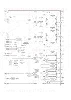
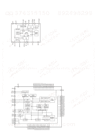
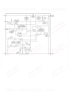
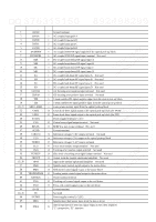
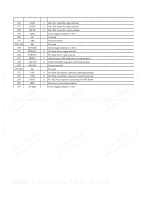
TEL 13942296513 QQ 376315150 892498299 TEL 13942296513 QQ 376315150 892498299 http://www.xiaoyu163.com HCD-DH3/DH5BT/DH7BT QQ 376315150 Pin No. Pin Name I/O 892498299 Description 115 RD7 I/O Two-way data bus with the SD-RAM 116 DVSS - Ground terminal 117, 118 RD6, RD5 I/O Two-way data bus with the SD-RAM 119 DVSS - Ground terminal 120, 121 RD4, RD3 I/O Two-way data bus with the SD-RAM 122 DVDD18 - Power supply terminal (+1.8V) 123 to 126 RD2 to RD0, RD15 I/O Two-way data bus with the SD-RAM 127 DVDD3 - Power supply terminal (+3.3V) 128 to 133 RD14 to RD9 I/O Two-way data bus with the SD-RAM 134 DVSS - Ground terminal 135 RD8 I/O Two-way data bus with the SD-RAM 136 GPIO - Not used 137 DQM1 O Data mask signal output to the SD-RAM 138 RWE O Write enable signal output to the SD-RAM 139 CAS O Column address strobe signal output to the SD-RAM 140 RAS O Row address strobe signal output to the SD-RAM 141 DVDD3 - Power supply terminal (+3.3V) 142 RCS O Chip select signal output to the SD-RAM 143 BA0 O Bank address signal output to the SD-RAM 144 DVSS - Ground terminal 145 BA1 O Bank address signal output to the SD-RAM TEL 13942296513 QQ 376315150 892498299 146, 147 148 RA10, RA0 DVSS O Address signal output to the SD-RAM - Ground terminal 149 to 151 RA1 to RA3 O Address signal output to the SD-RAM 152 DVDD18 - Power supply terminal (+1.8V) 153, 154 NC - Not used 155 DVDD3 - Power supply terminal (+3.3V) 156 RCLK O Serial data transfer clock signal output to the SD-RAM 157 CKE O Clock enable signal output to the SD-RAM 158 to 160 RA11, RA9, RA8 O Address signal output to the SD-RAM 161 DVSS - Ground terminal 162 RA7 O Address signal output to the SD-RAM 163 DVSS - Ground terminal 164 to 166 RA6 to RA4 O Address signal output to the SD-RAM 167 DVDD3 - Power supply terminal (+3.3V) 168 DISC/X - Not used 169 RGB - Not used 170 TSD_M O Thermal shut down signal output to the motor/coil driver 171, 172 NC - Not used 173 DVDD18 - Power supply terminal (+1.8V) 174 FWD O Loading motor drive signal output to the motor driver (forward direction) 175 NC - Not used www. xiaoyu163. com 176 LIMSW I Limit detection switch input terminal 177 OCSW I Disc in/out detection switch input terminal 178 REV O Loading motor drive signal output to the motor driver (reverse direction) 179 CKSW I Chucking detection switch input terminal 180, 181 NC - Not used 67 http://www.xiaoyu163.com
-
 1
1 -
2
-
3
-
4
-
5
-
6
-
7
-
8
-
9
-
10
-
11
-
12
-
13
-
14
-
15
-
16
-
17
-
18
-
19
-
20
-
21
-
22
-
23
-
24
-
25
-
26
-
27
-
28
-
29
-
30
-
31
-
32
-
33
-
34
-
35
-
36
-
37
-
38
-
39
-
40
-
41
-
42
-
43
-
44
-
45
-
46
-
47
-
48
-
49
-
50
-
51
-
52
-
53
-
54
-
55
-
56
-
57
-
58
-
59
-
60
-
61
-
 62
62 -
 63
63 -
 64
64 -
 65
65 -
 66
66 -
 67
67 -
 68
68 -
 69
69 -
 70
70 -
 71
71 -
 72
72 -
73
-
74
-
75
-
76
-
77
-
78
-
79
-
80
-
81
-
82
-
83
-
84
-
85
-
86
-
87
-
88
-
89
-
90
-
91
-
92
-
93
-
94
-
95
-
96
-
97
-
98
-
99
-
100
-
101
-
102
-
103
-
104
-
105
-
106
-
107
-
108
-
109
-
110
-
111
-
112
-
113
-
114
-
115
-
116
-
117
-
118
-
119
-
120
-
121
-
122
-
123
-
124
-
125
-
126
-
127
-
128
-
129
-
130
 |
 |