Sony HCD-DH7BT Service Manual - Page 70
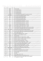
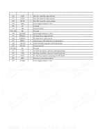
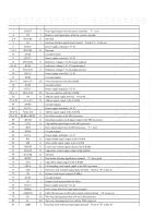
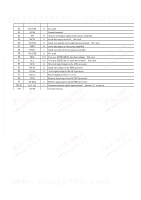
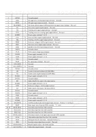
USB BOARD, IC901, TMP92CD28AFG-6UJ5 USB CONTROLLER, Pin No., Pin Name, Description
 |
View all Sony HCD-DH7BT manuals
Add to My Manuals
Save this manual to your list of manuals |
Page 70 highlights
HCD-DH3/DH5BT/DH7BT http://www.xiaoyu163.com TEL 13942296513 QQ 376315150 892498299 TEL 13942296513 QQ 376315150 892498299 QQ 376315150 USB BOARD IC901 TMP92CD28AFG-6UJ5 (USB CONTROLLER) 892498299 Pin No. Pin Name I/O Description 1 /RESET I Reset signal input from the system controller "L": reset 2 DI I Ready to send signal input from the system controller 3, 4 NO USE O Not used 5 G-3 I Function selection signal input terminal Fixed at "L" in this set 6 DVCC - Power supply terminal (+3.3 V) 7 to 9 NO USE O Not used 10 DVSS - Ground terminal 11 DVCC - Power supply terminal (+3.3 V) 12 RVOUT1 O Reference voltage (+3.3 V) output terminal 13, 14 RVIN I Reference voltage (+3.3 V) input terminal 15 RVOUT2 O Reference voltage (+3.3 V) output terminal 16 DVCC - Power supply terminal (+3.3 V) 17 DVSS - Ground terminal 18 to 25 D0 to D7 I/O Two-way data bus with the S-RAM 26 DVSS - Ground terminal 27 DVCC - Power supply terminal (+3.3 V) 28 to 35 D8 to D15 I/O Two-way data bus with the S-RAM 36 A0 O Address signal output terminal Not used 37 to 43 A1 to A7 O Address signal output to the S-RAM TEL 13942296513 QQ 376315150 892498299 44 DVSS - Ground terminal 45 DVCC - Power supply terminal (+3.3 V) 46 to 54 A8 to A16 O Address signal output to the S-RAM 55 to 58 BUS0 to BUS3 O Serial data output to the MP3 processor 59 /BUCK O Serial data transfer clock signal output to the MP3 processor 60 /CCE O Chip enable signal output to the MP3 processor 61 /RST I Reset signal input from the MP3 processor "L": reset 62 DVSS - Ground terminal 63 DVCC - Power supply terminal (+3.3 V) 64 RD O Output enable signal output to the S-RAM 65 WR O Write enable signal output to the S-RAM 66 SRLLB O Lower-byte control signal output to the S-RAM 67 SRLUB O Upper-byte control signal output to the S-RAM 68 NO USE O Not used 69 BOOT I Boot mode selection signal input terminal "L": boot mode 70 CS2 I Chip select signal output to the S-RAM 71 LRCK O L/R sampling clock signal output to the MP3 processor 72 AM1 I Function mode selection signal input terminal Fixed at "H" in this set 73 X2 O System clock output terminal (9 MHz) 74 DVSS - Ground terminal 75 X1 I System clock input terminal (9 MHz) 76 DVCC - Power supply terminal (+3.3 V) www. xiaoyu163. com 77 USBOC I Over current detection signal input terminal 78 USBPON O USB VBUS power on/off control signal output terminal "H": power on 79 D+ I/O Two-way data (positive) bus with the USB connector 80 D- I/O Two-way data (negative) bus with the USB connector 81 AM0 I Function mode selection signal input terminal Fixed at "H" in this set 70 http://www.xiaoyu163.com
-
 1
1 -
2
-
3
-
4
-
5
-
6
-
7
-
8
-
9
-
10
-
11
-
12
-
13
-
14
-
15
-
16
-
17
-
18
-
19
-
20
-
21
-
22
-
23
-
24
-
25
-
26
-
27
-
28
-
29
-
30
-
31
-
32
-
33
-
34
-
35
-
36
-
37
-
38
-
39
-
40
-
41
-
42
-
43
-
44
-
45
-
46
-
47
-
48
-
49
-
50
-
51
-
52
-
53
-
54
-
55
-
56
-
57
-
58
-
59
-
60
-
61
-
62
-
63
-
64
-
 65
65 -
 66
66 -
 67
67 -
 68
68 -
 69
69 -
 70
70 -
 71
71 -
 72
72 -
 73
73 -
 74
74 -
 75
75 -
76
-
77
-
78
-
79
-
80
-
81
-
82
-
83
-
84
-
85
-
86
-
87
-
88
-
89
-
90
-
91
-
92
-
93
-
94
-
95
-
96
-
97
-
98
-
99
-
100
-
101
-
102
-
103
-
104
-
105
-
106
-
107
-
108
-
109
-
110
-
111
-
112
-
113
-
114
-
115
-
116
-
117
-
118
-
119
-
120
-
121
-
122
-
123
-
124
-
125
-
126
-
127
-
128
-
129
-
130
 |
 |
