Sony STR-DB1070 Service Manual - Page 44
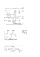
DIGITAL BOARD, IC1408, LC89056W-E DIGITAL AUDIO INTERFACE RECEIVER, Pin No., Pin Name, Description
 |
View all Sony STR-DB1070 manuals
Add to My Manuals
Save this manual to your list of manuals |
Page 44 highlights
STR-DB870/DB1070 • DIGITAL BOARD IC1408 LC89056W-E (DIGITAL AUDIO INTERFACE RECEIVER) Pin No. 1 2 3 4 5 6 7 8 9 10 11 12 13 14 Pin Name DISEL DOUT DIN0 DIN1 DIN2 DGND DVDD R VIN LPF AVDD AGND CKOUT BCK I/O Description I Input data select terminal (fixed at "L") O EIAJ data and parity output terminal Not used (open) I Amp integrate data input from the select switch (IC1406) O Amp integrate data input terminal Not used (fixed at "L") I Amp integrate data input terminal Not used (fixed at "L") - Ground terminal (for digital) - Power supply terminal (+5V) (for digital) I Input terminal for VCO generator band adjustment I Input terminal for VCO self running frequency set O External LPF for PLL is connected to this terminal - Power supply terminal (+5V) (for analog) - Ground terminal (for analog) O Clock signal output to the audio DSP1, 2 (IC1501, 1601) O Bit clock signal output to the A/D converter (IC1101) and audio DSP1 (IC1501) 15 LRCK O L/R sampling clock signal output to the A/D converter (IC1101) and audio DSP1, 2 (IC1501, 1601) 16 DATAO O Audio data output to the system controller (IC1703) and audio DSP1 (IC1501) 17 XSTATE O Clock status flag output to the system controller (IC1703) 18 DGND - Ground terminal (for digital) 19 DVDD - Power supply terminal (+5V) (for digital) 20 XMCK O Clock signal outout to the A/D converetr (IC1101) (24.576MHz) 21 XOUT O Clock output terminal Not used (open) 22 XIN I Clock input from the clock oscillator (IC1410) (24.576MHz) 23 EMPHA O Emphasis monitor output terminal "H": on Not used (open) 24 AUDIO O Audio transfer signal output to the audio DSP1 (IC1501) 25 CSFLAG O Not used (open) 26 to 29 F0/P0/C0 to F3/P3/C3 O Terminal for check Not used (open) 30 DVDD - Power supply terminal (+5V) (for digital) 31 DGND - Ground terminal (for digital) 32 AUTO O Not used (open) 33 BPSYNC O Not used (open) 34 ERROR O Error mute output to the system controller (IC1703) and audio DSP1 (IC1501) 35 DO O Data output to the system controller (IC1703) 36 DI I Data input from the system controller (IC1703) 37 CE I Chip enable signal input from the system controller (IC1703) 38 CLK I Clock signal input from the system controller (IC1703) 39 XSEL I Clock select terminal (fixed at "H") 40, 41 MODE0, MODE1 I Mode setting input terminal (fixed at "L") 42 DGND - Ground terminal (for digital) 43 DVDD - Power supply terminal (+5V) (for digital) 44, 45 DOSEL0, DOSEL1 I Data format select signal input terminal (fixed at "L") 46 CKSEL0 I System clock select signal input terminal (fixed at "L") 47 CKSEL1 I System clock select signal input from the system controller (IC1703) 48 XMODE I Reset signal input from the system controller (IC1703) 44
-
 1
1 -
2
-
3
-
4
-
5
-
6
-
7
-
8
-
9
-
10
-
11
-
12
-
13
-
14
-
15
-
16
-
17
-
18
-
19
-
20
-
21
-
22
-
23
-
24
-
25
-
26
-
27
-
28
-
29
-
30
-
31
-
32
-
33
-
34
-
35
-
36
-
37
-
38
-
 39
39 -
 40
40 -
 41
41 -
 42
42 -
 43
43 -
 44
44 -
 45
45 -
 46
46 -
 47
47 -
 48
48 -
 49
49 -
50
-
51
-
52
-
53
-
54
-
55
-
56
-
57
-
58
-
59
-
60
-
61
-
62
-
63
-
64
-
65
-
66
-
67
-
68
-
69
-
70
-
71
-
72
-
73
-
74
-
75
-
76
-
77
-
78
-
79
-
80
-
81
-
82
-
83
-
84
-
85
-
86
 |
 |
