Sony STR-DB1070 Service Manual - Page 45
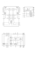
Digital Board, Ic1501, Cdx9617r Audio Dsp1
 |
View all Sony STR-DB1070 manuals
Add to My Manuals
Save this manual to your list of manuals |
Page 45 highlights
STR-DB870/DB1070 • DIGITAL BOARD IC1501 CDX9617R (AUDIO DSP1) Pin No. 1 2 3 4 5 6 7 8 9 10 11 12 13 14 15 16 17 18 19 20 21 22 23 to 26 27 28 29 30 31 32 33 34 35 36 37 38 39 40 41 42 43 44 45 46 47 48 Pin Name VSS XRST EXTIN FS2 VDDI FS1 PLOCK VSS MCLK1 VDDI VSS MCLK2 MS SCKOUT LRCKI1 VDDE BCKI1 SDI1 LRCKO BCKO VSS KFSIO SDO1 to SDO4 SPDIF LRCKI2 BCKI2 SDI2 VSS HACN HDIN HCLK HDOUT HCS SDCLK CLKEN RAS VDDI VSS CAS DQM/OE0 CS0 WE0 VDDE WMD1 VSS I/O Description - Ground terminal I Reset signal input from the system controller (IC1703) I Master clock input terminal Not used (fixed at "L") I Sampling frequency select signal input terminal Not used (fixed at "L") - Power supply terminal (+2.5V) I Sampling frequency select signal input terminal Not used (fixed at "L") O Internal PLL lock signal output terminal Not used (open) - Ground terminal I Systen clock input terminal (13.5MHz) - Power supply terminal (+2.5V) - Ground terminal O Systen clock output terminal (13.5MHz) I Master/slave active select terminal "L": internal clock, "H": external clock O Internal system clock output terminal Not used (open) I L/R sampling clock signal input from the audio interface receiver (IC1408) - Power supply terminal (+3.3V) I Bit clock signal input from the audio interface receiver (IC1408) I Audio data input from the A/D converter (IC1503) O L/R sampling clock signal output to the audio DSP2 (IC1601) O Bit clock signal output to the audio DSP2 (IC1601) - Ground terminal I/O Audio clock signal (384fs/256fs) in/out terminal O Audio serial data output to the audio DSP2 (IC1601) O S/PDIF output terminal Not used (open) I L/R sampling clock signal input from the audio interface receiver (IC1408) I Bit clock signal input from the audio interface receiver (IC1408) I Audio serial data input from the audio interface receiver (IC1408) - Ground terminal O Host acknowledge signal output to the system controller (IC1703) I Host serial data input from the system contrller (IC1703) I Host clock signal input from the system contrller (IC1703) O Host serial data output to the system contrller (IC1703) I Host chip select input from the system contrller (IC1703) O SD-RAM clock output terminal Not used (open) O SD-RAM clock enable output terminal Not used (open) O Row address strobe signal output terminal Not used (open) - Power supply terminal (+2.5V) - Ground terminal O Column address strobe signal output terminal Not used (open) O Mask data output terminal O Chip select isignal output to the S-RAM (IC1502) O Write enable signal output to the S-RAM (IC1502) - Power supply terminal (+3.3V) I External memory wait mode setting terminal (fixed at "H") - Ground terminal 45
-
 1
1 -
2
-
3
-
4
-
5
-
6
-
7
-
8
-
9
-
10
-
11
-
12
-
13
-
14
-
15
-
16
-
17
-
18
-
19
-
20
-
21
-
22
-
23
-
24
-
25
-
26
-
27
-
28
-
29
-
30
-
31
-
32
-
33
-
34
-
35
-
36
-
37
-
38
-
39
-
 40
40 -
 41
41 -
 42
42 -
 43
43 -
 44
44 -
 45
45 -
 46
46 -
 47
47 -
 48
48 -
 49
49 -
 50
50 -
51
-
52
-
53
-
54
-
55
-
56
-
57
-
58
-
59
-
60
-
61
-
62
-
63
-
64
-
65
-
66
-
67
-
68
-
69
-
70
-
71
-
72
-
73
-
74
-
75
-
76
-
77
-
78
-
79
-
80
-
81
-
82
-
83
-
84
-
85
-
86
 |
 |
