Sony STR-DB1070 Service Manual - Page 51
Sony STR-DB1070 - Fm Stereo/fm-am Receiver Manual
 |
View all Sony STR-DB1070 manuals
Add to My Manuals
Save this manual to your list of manuals |
Page 51 highlights
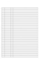
STR-DB870/DB1070 Pin No. Pin Name I/O Description 41 M STATUS O STATUS (M BUS) control signal output to the select switch (IC751) 42 D.POWER O Power ON/OFF control signal output terminal (digital section power) 43 V.POWER O Power ON/OFF control signal output terminal (video section power) 44 VSS - Ground terminal 45, 46 NC I Not used (fixed at "L" ) 47 ERROR I Error signal input from the audio DSP (IC1601) 48 NC I Not used (fixed at "L" ) 49 SUB.T.PORT O Sub power transformer (T2) on/off signal output terminal 50 AUDIO SPLIT LED O LED drive signal output of AUDIO SPLIT indicator (D1801) 51 GND - Not used (fixed at "L" ) 52 MD2 O MD2 signal output terminal (fixed at "L" ) 53 MD1 O MD1 signal output terminal (fixed at "H" ) 54 MD0 O MD0 signal output terminal (fixed at "H" ) 55 RSTX I System reset signal input from the reset signal generator (IC1702) 56 VCC - Power supply terminal (+3.3V) 57 X1 O Main system clock output terminal (16.5MHz) 58 X0 I Main system clock output terminal (16.5MHz) 59 VSS - Ground terminal 60 STOP I AC power check signal input terminal 61 RDS CLK I RDS serial data transfer clock signal input from the RDS decoder (IC1303) 62 POWER I Key input terminal I/1 key (S1704) input 63 MBUS TV I TV (M BUS) signal input from the TV jack (J755) (US, Canadian models only) 64 MBUS DVD I DVD (M BUS) signal input terminal (US, Canadian models only) 65 MBUS VIDEO I VIDEO (M BUS) input terminal (US, Canadian models only) 66 SIRCS I Sircs signal input from the remote control receiver (IC1701) and select switch (IC751) 67 DIR ERROR I Error signal input from the digital audio interface receiver (IC1408) 68 VCC - Power supply terminal (+3.3V) 69 XSTATE I Clock status flag signal input from the digital audio interface receiver (IC1408) 70 DATA0 I Audio data input from the digital audio interface receiver (IC1408) 71 XMODE O Reset signal output to the digital audio interface receiver (IC1408) "L": active 72 CKSEL1 O System clock select 1 output to the digital audio interface receiver (IC1408) 73 CLK O Clock signal output to the digital audio interface receiver (IC1408) 74 CE O Chip enable signal output to the digital audio interface receiver (IC1408) 75 DI O Data output to the digital audio interface receiver (IC1408) 76 DO I Data input from the digital audio interface receiver (IC1408) 77 VCC - Power supply terminal (+3.3V) 78 BST O Booster control signal output to the audio DSP2 (IC1601) 79 PM2 O PLL initialize signal output to the audio DSP2 (IC1601) 80 XRST2 O Reset signal output to the audio DSP2 (IC1601) 81 HACN2 I Host acknowledge signal input from the audio DSP2(IC1601) 82 HCS2 O Host chip select signal output to the audio DSP2 (IC1601) 83 GB9 I Signal input from the audio DSP1 (IC1501) 84 BST1 O Boot strap signal output to the audio DSP1 (IC1501) 85 HCS1 O Host chip select signal output to the audio DSP1 (IC1501) 86 A1 IN I Audio bus input terminal (control A1) 87 A1 OUT O Audio bus output terminal (control A1) 51
-
 1
1 -
2
-
3
-
4
-
5
-
6
-
7
-
8
-
9
-
10
-
11
-
12
-
13
-
14
-
15
-
16
-
17
-
18
-
19
-
20
-
21
-
22
-
23
-
24
-
25
-
26
-
27
-
28
-
29
-
30
-
31
-
32
-
33
-
34
-
35
-
36
-
37
-
38
-
39
-
40
-
41
-
42
-
43
-
44
-
45
-
 46
46 -
 47
47 -
 48
48 -
 49
49 -
 50
50 -
 51
51 -
 52
52 -
 53
53 -
 54
54 -
 55
55 -
 56
56 -
57
-
58
-
59
-
60
-
61
-
62
-
63
-
64
-
65
-
66
-
67
-
68
-
69
-
70
-
71
-
72
-
73
-
74
-
75
-
76
-
77
-
78
-
79
-
80
-
81
-
82
-
83
-
84
-
85
-
86
 |
 |