Sony STR-DB1070 Service Manual - Page 54
Video Board, Ic307, Mb90089f-g-238-bnd Osd Driver
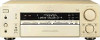 |
View all Sony STR-DB1070 manuals
Add to My Manuals
Save this manual to your list of manuals |
Page 54 highlights
STR-DB870/DB1070 • VIDEO BOARD IC307 MB90089F-G-238-BND (OSD DRIVER) Pin No. 1 2 3 4 5 6 7 Pin Name YIN CIN VIN AVCC FSCO VBLK VCC I/O Description I Y (luminance) signal input from the Y switch (IC752) I C (color) signal input from the C switch (IC750) I Composite video signal input from the video select (IC308) - Power supply terminal (+5V) (for analog) O Internal color burst phase display signal output terminal Not used (open) O Vertical blanking timing signal output terminal Not used (open) - Power supply terminal (+5V) 8 EXS I External clock generator circuit for color burst (NTSC: 14.31818MHz, PAL: 17.734475MHz) 9 XS O Clock signal output terminal for color burst Not used (open) 10 HSYNC O Horizontal synchronizing signal output terminal (for test) 11 VSYNC O Vertical synchronizing signal output terminal (for test) 12 EXHSYN I External horizontal synchronizing signal input terminal Not used (open) 13 EXVSYN I External vertical synchronizing signal input terminal Not used (open) 14 VSS - Ground terminal 15 EXD I Dot clock generator connecting terminal for display 16 XD O Dot clock generator connecting terminal for display 17 VOB O Blanking signal output terminal Not used (open) 18 VOC2 O color signal output terminal Not used (open) 19 VOC1 O color signal output terminal Not used (open) 20 VOC0 O color signal output terminal Not used (open) 21 TEST I Test signal input terminal "L": test (normally: fixed at "H") 22 SCLK I Serial data transfer shift clock signal input terminal 23 SIN I Serial data input terminal 24 CS I Chip select signal input terminal "L": active 25 VOUT O Composite video signal output to the video buffer (IC305) 26 COUT O C (color) signal output to the video buffer (IC305) 27 YOUT O Y (luminance) signal output to the video buffer (IC305) 28 AVSS - Ground terminal (for analog) 54
-
 1
1 -
2
-
3
-
4
-
5
-
6
-
7
-
8
-
9
-
10
-
11
-
12
-
13
-
14
-
15
-
16
-
17
-
18
-
19
-
20
-
21
-
22
-
23
-
24
-
25
-
26
-
27
-
28
-
29
-
30
-
31
-
32
-
33
-
34
-
35
-
36
-
37
-
38
-
39
-
40
-
41
-
42
-
43
-
44
-
45
-
46
-
47
-
48
-
 49
49 -
 50
50 -
 51
51 -
 52
52 -
 53
53 -
 54
54 -
 55
55 -
 56
56 -
 57
57 -
 58
58 -
 59
59 -
60
-
61
-
62
-
63
-
64
-
65
-
66
-
67
-
68
-
69
-
70
-
71
-
72
-
73
-
74
-
75
-
76
-
77
-
78
-
79
-
80
-
81
-
82
-
83
-
84
-
85
-
86
 |
 |
