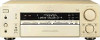
Sony STR-DB1070 Service Manual - Page 48
Sony STR-DB1070 - Fm Stereo/fm-am Receiver Manual
 |
View all Sony STR-DB1070 manuals
Add to My Manuals
Save this manual to your list of manuals |
Page 48 highlights
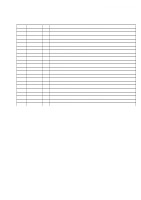
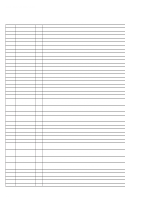
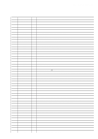
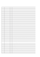
STR-DB870/DB1070 Pin No. 60, 61 62 63 64 65 66 67, 68 69, 70 71 72 73 74 75 76 77, 78 79 80 81 82 83 84 85 86 87 to 89 90 91 92 to 94 95 96 97 98 99 100 101 102 103, 104 105, 106 107, 108 109 110 111 112 113, 114 115, 116 117 118, 119 Pin Name SDO1, SDO2 KFSIO LRCKO BCKO VDDI VSS D18, D17 A10, A9 CAS RAS VDDI HDIN HCLK HCS A8, A7 D16 D15 VSS HDOUT HACN CSO WEO A6 D14 to D12 VDDE VSS D11 to D9 A5 VDDI TCK TDI TDO TMS XTRST VSS D8, D7 A4, A3 GP10, GP9 VDDI GP8 GP7 GP6 A2, A1 D6, D5 VSS GP5, GP4 48 I/O Description O Audio serial data output to the D/A converter (IC1201) I/O Audio clock signal (384fs/256fs) in/out terminal O L/R sampling clock signal output to the D/A converter (IC1201, 1202) O Bit clock signal output to the D/A converter (IC1201, 1202) - Power supply terminal (+2.5V) - Ground terminal I/O Two-way data bus with the S-RAM (IC1602) O Address signal output to the S-RAM (IC1602) O Column address strobe signal output terminal Not used (open) O Row address strobe signal output terminal Not used (open) - Power supply terminal (+2.5V) I Host serial data input from the system contrller (IC1703) I Host clock signal input from the system contrller (IC1703) I Host chip select input from the system contrller (IC1703) O Address signal output to the S-RAM (IC1602) I/O Two-way data bus with the S-RAM (IC1602) I/O Two-way data bus terminal Not used (open) - Ground terminal O Host serial data input from the system contrller (IC1703) O Host acknowledge signal output to the system controller (IC1703) O Chip select signal output to the S-RAM (IC1602) O Write enable signal output to the S-RAM (IC1602) O Address signal output to the S-RAM (IC1602) I/O Two-way data bus terminal Not used (open) - Power supply terminal (+3.3V) - Ground terminal I/O Two-way data bus terminal Not used (open) O Address signal output to the S-RAM (IC1602) - Power supply terminal (+2.5V) I Emulation clock signal input terminal Not used (open) I Emulation data input terminal Not used (open) O Emulation data input terminal Not used (open) I Emulation data input start/end select Not used (open) I Emulation break signal input terminal Not used (open) - Ground terminal I/O Two-way data bus terminal Not used (open) O Address signal output to the S-RAM (IC1602) - Not used (open) - Power supply terminal (+2.5V) - Not used (open) I Serial clock signal input terminal - Not used (open) O Address signal output to the S-RAM (IC1602) I/O Two-way data bus terminal Not used (open) - Ground terminal - Not used (open)
-
 1
1 -
2
-
3
-
4
-
5
-
6
-
7
-
8
-
9
-
10
-
11
-
12
-
13
-
14
-
15
-
16
-
17
-
18
-
19
-
20
-
21
-
22
-
23
-
24
-
25
-
26
-
27
-
28
-
29
-
30
-
31
-
32
-
33
-
34
-
35
-
36
-
37
-
38
-
39
-
40
-
41
-
42
-
 43
43 -
 44
44 -
 45
45 -
 46
46 -
 47
47 -
 48
48 -
 49
49 -
 50
50 -
 51
51 -
 52
52 -
 53
53 -
54
-
55
-
56
-
57
-
58
-
59
-
60
-
61
-
62
-
63
-
64
-
65
-
66
-
67
-
68
-
69
-
70
-
71
-
72
-
73
-
74
-
75
-
76
-
77
-
78
-
79
-
80
-
81
-
82
-
83
-
84
-
85
-
86
 |
 |
