Sony STR-DB1070 Service Manual - Page 47
Digital Board, Ic1601, Cxd9616r Audio Dsp2,
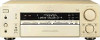 |
View all Sony STR-DB1070 manuals
Add to My Manuals
Save this manual to your list of manuals |
Page 47 highlights
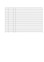
STR-DB870/DB1070 • DIGITAL BOARD IC1601 CXD9616R (AUDIO DSP2) Pin No. Pin Name I/O 1 VDDI - 2 EXTIN I 3, 4 WMD1, WMD0 I 5 MOD1 I 6 MOD0 I 7 VSS - 8 XRST I 9 VSS - 10 SCKOUT O 11 VDDI (PLL) - 12 SYNC I 13 to 15 PAGE2 to PAGE0 O 16 PLOCK O 17 BTACK I 18 VDDE - 19 VSS - 20 to 22 D31 to D29 I/O 23 A17 O 24 VSS - 25 SDO3 O 26 SDO4 O 27, 28 SDI1, SDI2 I 29 LRCKI1 I 30 VSS - 31, 32 D28, D27 I/O 33 A16 O 34 A15 O 35 SDI3 I 36 L2 - 37 VDDI - 38 BCKI1 I 39 SDI4 I 40 MS I 41, 42 A14, A13 O 43, 44 D26, D25 I/O 45 VSS - 46 BCKI2 I 47, 48 FS2, FS1 I 49 SPDIF I 50 A12 O 51 to 53 D24 to D22 I/O 54 VDDE - 55 VSS - 56 to 58 D21 to D19 I/O 59 A11 O Description Power supply terminal (+2.5V) Not used (fixed at "L") External memory wait mode setting terminal (fixed at "H") Mode select signal input terminal "L": 384fs, "H": 256fs Mode select signal input terminal "L": single chip mode, "H": can not use Ground terminal Reset signal input from the system controller (IC1703) Ground terminal Serial clock signal output to the D/A converter (IC1201, 1202) Power supply terminal (+2.5V) (for PLL) Sync/unsync select signal input terminal "L": sync External memory page select signal output terminal Not used (open) Internal PLL lock signal output teminal Not used (open) Boot mode display signal output teminal Not used (open) Power supply terminal (+3.3V) Ground terminal Two-way data bus with the S-RAM (IC1602) Address signal output terminal Not used (open) Ground terminal Audio serial data output to the D/A converter (IC1201) Audio serial data output to the D/A converter (IC1202) Audio serial data input from the audio DSP1 (IC1501) L/R sampling clock signal input from the audio DSP1 (IC1501) Ground terminal Two-way data bus with the S-RAM (IC1602) Address signal output terminal Not used (open) Address signal output to the S-RAM (IC1602) Audio serial date input from the audio DSP1 (IC1501) Not used (open) Power supply terminal (+2.5V) Bit clock signal input from the audio DSP1 (IC1501) Audio serial data input from the audio DSP1 (IC1501) Master/slave active select terminal "L": internal clock, "H": external clock (fixed at "L") Address signal output to the S-RAM (IC1602) Two-way data bus with the S-RAM (IC1602) Ground terminal Bit clock signal input terminal Not used (open) Sampling frequency select signal input terminal Not used (open) S/PDIF output terminal Not used (open) Address signal output to the S-RAM (IC1602) Two-way data bus with the S-RAM (IC1602) Power supply terminal (+3.3V) Ground terminal Two-way data bus with the S-RAM (IC1602) Address signal output to the S-RAM (IC1602) 47
-
 1
1 -
2
-
3
-
4
-
5
-
6
-
7
-
8
-
9
-
10
-
11
-
12
-
13
-
14
-
15
-
16
-
17
-
18
-
19
-
20
-
21
-
22
-
23
-
24
-
25
-
26
-
27
-
28
-
29
-
30
-
31
-
32
-
33
-
34
-
35
-
36
-
37
-
38
-
39
-
40
-
41
-
 42
42 -
 43
43 -
 44
44 -
 45
45 -
 46
46 -
 47
47 -
 48
48 -
 49
49 -
 50
50 -
 51
51 -
 52
52 -
53
-
54
-
55
-
56
-
57
-
58
-
59
-
60
-
61
-
62
-
63
-
64
-
65
-
66
-
67
-
68
-
69
-
70
-
71
-
72
-
73
-
74
-
75
-
76
-
77
-
78
-
79
-
80
-
81
-
82
-
83
-
84
-
85
-
86
 |
 |
