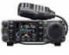
Icom IC-7000 Service Manual - Page 10
2nd Mixer Circuit Main Unit, L8, L10-l13, C18, C25, C26, C28, C29, C31-c33 Via
 |
View all Icom IC-7000 manuals
Add to My Manuals
Save this manual to your list of manuals |
Page 10 highlights
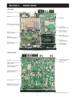
3-2-5 2ND MIXER CIRCUIT (MAIN UNIT) The 2nd mixer circuit mixes the 2nd IF signal with the 2nd LO signal to convert into the 1st IF frequency. 3-2-8 RF CIRCUIT (MAIN UNIT) The RF circuit amplifies and filters the RF signal from the 1st mixer circuit. The filtered signal from the bandpass filter (FI901) is applied to the 2nd mixer circuit (D801) and mixed with 2nd LO signal (124.032 MHz) to convert into the 1st IF signal. The HF/50 MHz bands signal from the 1st mixer circuit (IC401) is passed through the low-pass filter (L310, L312, C314, C316, C318, C320, C322) via the band switch (D305). The 2nd LO signal is generated in the DDS unit, and applied to the 2nd mixer circuit (D801) after being filtered and attenuated at the low-pass filter (L808, C816, C817) and the attenuators (R801, R805, R806, R809-R811), respectively. The converted 1st IF signal is applied to the 1st IF circuit. The HF band signal is passed through one of 5 high-pass (Refer to 3-1 for used RF high-pass filter) and low-pass (L205, L207, C209-C213) filters. The 50 MHz band signal is passed through the bandpass filter (L219, L220, L246-L248, C240-C242, C282, C285- C291). 3-2-6 1ST IF CIRCUIT (MAIN UNIT) The 1st IF circuit amplifies and filters the 1st IF signal. The converted 1st IF signal is applied to the IF amplifier (Q701) via the TX switch (D703) and then passed through the bandpass filter (FI601) to suppress unwanted signals via the filter switches (D601, D602). The filtered HF/50 MHz bands signal is amplified at the YGR amplifier (IC1) after passed through the high-pass filter (L109, L110, L116, L117, C109, C114-C116) and attenuator (R5- R7). The amplified HF/50 MHz bands signal is applied to the drive and power amplifier circuits (PA unit) via J1. The filtered signals are applied to the 1st mixer circuit. 3-2-7 1ST MIXER CIRCUIT (MAIN UNIT) The 1st mixer circuit mixes the 1st IF signal with the 1st LO signal to convert into the RF frequency. The filtered signal is applied to the 1st mixer circuit (IC401) via the TX switches (D501, D504) and mixed with the 1st LO signal (124.517-594.487 MHz) to convert into the RF signal. The 1st LO signal is generated in the DDS unit, and applied to the 1st mixer circuit (IC401, pins 1, 6) after being amplified and attenuated at the 1st LO amplifier (IC421, pins 1, 4) and the attenuators (R416-R418, R421-R423), respectively. The converted RF signal is applied to the RF circuit. The VHF/UHF bands signal from the 1st mixer circuit (IC401) is passed through the low-pass filter (L309, L311, L313, C313, C315, C317, C319, C321, C323, C325) via the band switch (D306). The VHF band signal is passed through the bandpass filter (L8, L10-L13, C18, C25, C26, C28, C29, C31-C33) via the band switches (D3, D10) and then amplified at the RF amplifier (IC2, pins 1, 3). The amplified signal is passed through the band switch (D1) and attenuator (R5-R7), and then applied to the YGR amplifier (IC1, pins 1, 4). The amplified signal is passed through the high pass filter (L21, C50-C52) via the filter switches (D6, D8) and then applied to the drive and power amplifier circuits (PA unit) via J1. The UHF band signal is amplified at the RF amplifier (IC3, pins 1, 3) via the band switch (D4) and passed through the bandpass filters (FI2, FI3). The filtered signal is amplified at the YGR amplifier (IC1, pins 1, 4) after passed through the band switch (D2), attenuator (R5-R7) and bypass switches (D7, D9). • TRANSMITTER CONSTRUCTION The amplified signal is applied to the drive and power amplifier circuits (PA unit) via J1. MIC Controller LOGIC UNIT (DSP circuit) A/D IC551 DSP ICs IC301 IC2201 D/A IC551 3rd LO (438.85 kHz) 455 kHz Q901 AMP. FI901 Ceramic BPF 124.487 MHz 2nd LO (124.032 MHz) 2nd mixer D801 ANT1 Q801 AMP. FI601 Crystal BPF MAIN UNIT 1st mixer IC401 HPFs 1st LO BPF (124.517− 594.487 MHz) AMP. PA UNIT Q301 HF/50 MHz PA Q302 LPFs IC504 DRIVER UNIT 145 MHz 430 MHz Q501 PA Q401 PA ANT2 3 - 5
-
 1
1 -
2
-
3
-
4
-
 5
5 -
 6
6 -
 7
7 -
 8
8 -
 9
9 -
 10
10 -
 11
11 -
 12
12 -
 13
13 -
 14
14 -
 15
15 -
16
-
17
-
18
-
19
-
20
-
21
-
22
-
23
-
24
-
25
-
26
-
27
-
28
-
29
-
30
-
31
-
32
-
33
-
34
-
35
-
36
-
37
-
38
-
39
-
40
-
41
-
42
-
43
-
44
-
45
-
46
-
47
-
48
-
49
-
50
-
51
-
52
-
53
-
54
-
55
-
56
-
57
-
58
-
59
-
60
-
61
-
62
-
63
-
64
-
65
-
66
-
67
-
68
-
69
-
70
-
71
-
72
-
73
-
74
-
75
-
76
-
77
-
78
-
79
-
80
-
81
-
82
-
83
-
84
-
85
-
86
-
87
-
88
-
89
-
90
-
91
-
92
 |
 |
