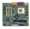
MSI MS 6378 User Guide - Page 48
Advanced Chipset Features
 |
View all MSI MS 6378 manuals
Add to My Manuals
Save this manual to your list of manuals |
Page 48 highlights
Chapter 3 Advanced Chipset Features The Advanced Chipset Features setup options are used to change the values of the chipset registers. These registers control most of the system options in the computer. CMOS Setup Utility - Copyright(C) 1984-2000 Award Software Advanced Chipset Features DRAM Timing by SPD x SDRAM Cycle Length x DRAM Clock Memory Hole P2C/C2P Concurrency Fast R-W Turn Around System BIOS Cacheable Video RAM Cacheable Frame Buffer Size AGP Aperture Size OnChip USB USB Keyboard Support OnChip Sound OnChip Modem CPU to PCI Write Buffer PCI Dynamic Bursting PCI Master 0 WS Write PCI Delay Transaction PCI#2 Access #1 Retry Yes Auto Auto Disabled Enabled Enabled Disabled Disabled 8M 64M Enabled Disabled Auto Auto Enabled Enabled Enabled Enabled Enabled Item Help Menu Level 8 AGP Master 1 WS Write AGP Master 1 WS Read Memory Parity/ECC Check Disabled Disabled Disabled Move Enter:Select +/-/PU/PD:Value F10:Save ESC:Exit F1:General Help F5:Previous Values F6:Fail-Safe Defaults F7:Optimized Defaults Note: Change these settings only if you are familiar with the chipset. DRAM Timing by SPD Selects whether DRAM timing is controlled by the SPD (Serial Presence Detect) EEPROM on the DRAM module. Setting to Yes enables SDRAM Cycle Length and DRAM Clock automatically to be determined by BIOS based on the configurations on the SPD. Selecting No allows users to configure these fields manually. 3-12
-
 1
1 -
2
-
3
-
4
-
5
-
6
-
7
-
8
-
9
-
10
-
11
-
12
-
13
-
14
-
15
-
16
-
17
-
18
-
19
-
20
-
21
-
22
-
23
-
24
-
25
-
26
-
27
-
28
-
29
-
30
-
31
-
32
-
33
-
34
-
35
-
36
-
37
-
38
-
39
-
40
-
41
-
42
-
 43
43 -
 44
44 -
 45
45 -
 46
46 -
 47
47 -
 48
48 -
 49
49 -
 50
50 -
 51
51 -
 52
52 -
 53
53 -
54
-
55
-
56
-
57
-
58
-
59
-
60
-
61
-
62
-
63
-
64
-
65
-
66
-
67
-
68
-
69
-
70
-
71
-
72
 |
 |
