Sharp KB-3300JS Service Manual - Page 31
Description Of Lsi Ic-1
 |
View all Sharp KB-3300JS manuals
Add to My Manuals
Save this manual to your list of manuals |
Page 31 highlights
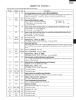
DESCRIPTION OF LSI (IC-1) KB-3300JS KB-3300JK KB-3300JW The I/O signal of the LSIis detailed in the following table. Pin No. Signal I/O Description 1 AN5 IN Temperature measurement input: OVEN THERMISTOR. By inputting DC voltage corresponding to the temperature detected by the thermistor, this input is converted into temperature by the A/D converter built into the LSI. 2 AN4 IN Turminal not used. 3 AN3 OUT Door lock motor driving signal. To turn on and off shut-off relay(RY8). "H"level during door lock motor driving "L" level otherwise ON During H: +5V door lock motor driving OFF L: GND 4 AN2 IN Input signal which communicates the oven door locked information to LSI. Door unlocked; "H" level signal(+5V). Door locked; "L" level signal(0V). 5 AN1 IN Input signal which communicates the oven door unlocked information to LSI. Door locked; "H" level signal(+5V). Door unlocked; "L" level signal(0V). 6 AN0 IN Turminal not used. 7 CNVSS IN Power source voltage: 0V (GND). VC voltage of power source circuit input. Connected GND. 8 RESET IN Auto clear terminal. Signal is input to reset the LSI to the initial state when power is applied. Temporarily set to "L" level the moment power is applied, at this time the LSI is reset. Thereafter set at "H" level. 9 P62 OUT Memory (EEPROM) clock out. 10 P61 IN/OUT Memory (EEPROM) data input/output. 11 VSS IN Power source voltage: 0V (GND). VS voltage of power source circuit input. Connected GND. 12 XIN IN Internal clock oscillation frequency setting input. The internal clock frequency is set by inserting the ceramic filter oscillation circuit with respect to Xout terminal. 13 XOUT OUT Internal clock oscillation frequency control output. Output to control oscillation input of Xin. 14 VCC IN Power source voltage: +5V. VC voltage of power source circuit input. 15 P60 OUT Turminal not used. 16 -19 P37- P34 OUT Turminal not used. 20 RXD2 IN Input terminal to check the data of display. Data signal from IC-3 is input to RXD2 to check the flow of the data. 21 TXD2 IN Output terminal to send IC-2 the data. The data of display is output to IC-2. 22 SCLK OUT Clock timing signaI output terminal. Clock timing signal is sent to IC-2 and IC-3. 23 P30 OUT Signal to reset LSI. Signal is output to reset IC-2, IC-3 and IC-4. 24 - 27 COM3 - COM0 OUT Turminal not used. 28 VL3 IN Connected VC (+5V). 29 - 34 P27- P22 OUT Turminal not used. 35 P21 OUT Turminal not used. 36 P20 OUT Turminal not used. 29
-
 1
1 -
2
-
3
-
4
-
5
-
6
-
7
-
8
-
9
-
10
-
11
-
12
-
13
-
14
-
15
-
16
-
17
-
18
-
19
-
20
-
21
-
22
-
23
-
24
-
25
-
 26
26 -
 27
27 -
 28
28 -
 29
29 -
 30
30 -
 31
31 -
 32
32 -
 33
33 -
 34
34 -
 35
35 -
 36
36 -
37
-
38
-
39
-
40
-
41
-
42
-
43
-
44
-
45
-
46
-
47
-
48
-
49
-
50
-
51
-
52
-
53
-
54
-
55
-
56
-
57
-
58
-
59
-
60
-
61
-
62
-
63
-
64
-
65
-
66
-
67
-
68
-
69
-
70
-
71
-
72
 |
 |
