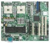
Intel SE7525RP2 Product Specification - Page 7

List of s - bios update

Page 7 highlights

Intel® Server Board SE7320EP2 / Intel® Server Board SE7525RP2 List of Figures 12.2.3 Ministry of Economic Development (New Zealand) Declaration of Conformity ... 130 12.2.4 BSMI (Taiwan) ...130 12.3 Replacing the Back up Battery 130 Appendix A: Integration and Usage Tips 131 Glossary...132 List of Figures Figure 1. Block Diagram of Intel® Server Boards SE7320EP2 and SE7525RP2 13 Figure 2. CEK 'Passive' Component Stackup 16 Figure 3. Memory Sub-system Block Diagram 17 Figure 4. Memory Bank Label Definition 19 Figure 5. Intel® Server Boards SE7320EP2 and SE7525RP2 SMBUS Block Diagram 28 Figure 6. Intel® Server Boards SE7320EP2 and SE7525RP2 Clock Distribution Diagram ....... 30 Figure 7. Video Controller PCI Bus Interface 35 Figure 8. Interrupt Routing Diagram 38 Figure 9. Interrupt Routing Diagram 39 Figure 10. BIOS Identification String 41 Figure 11. Fan Speed Control Block Diagram 82 Figure 12. System Recovery and Update Jumpers (J17 120 Figure 13. Output Voltage Timing 124 Figure 14. Turn On / Turn Off Timing 126 Revision 1.0 vii Intel order number D24635-001

  • 1
  • 2
  • 3
  • 4
  • 5
  • 6
  • 7
  • 8
  • 9
  • 10
  • 11
  • 12
  • 13
  • 14
  • 15
  • 16
  • 17
  • 18
  • 19
  • 20
  • 21
  • 22
  • 23
  • 24
  • 25
  • 26
  • 27
  • 28
  • 29
  • 30
  • 31
  • 32
  • 33
  • 34
  • 35
  • 36
  • 37
  • 38
  • 39
  • 40
  • 41
  • 42
  • 43
  • 44
  • 45
  • 46
  • 47
  • 48
  • 49
  • 50
  • 51
  • 52
  • 53
  • 54
  • 55
  • 56
  • 57
  • 58
  • 59
  • 60
  • 61
  • 62
  • 63
  • 64
  • 65
  • 66
  • 67
  • 68
  • 69
  • 70
  • 71
  • 72
  • 73
  • 74
  • 75
  • 76
  • 77
  • 78
  • 79
  • 80
  • 81
  • 82
  • 83
  • 84
  • 85
  • 86
  • 87
  • 88
  • 89
  • 90
  • 91
  • 92
  • 93
  • 94
  • 95
  • 96
  • 97
  • 98
  • 99
  • 100
  • 101
  • 102
  • 103
  • 104
  • 105
  • 106
  • 107
  • 108
  • 109
  • 110
  • 111
  • 112
  • 113
  • 114
  • 115
  • 116
  • 117
  • 118
  • 119
  • 120
  • 121
  • 122
  • 123
  • 124
  • 125
  • 126
  • 127
  • 128
  • 129
  • 130
  • 131
  • 132

Intel® Server Board SE7320EP2 / Intel® Server Board SE7525RP2
List of Figures
Revision 1.0
Intel order number D24635-001
vii
12.2.3
Ministry of Economic Development (New Zealand) Declaration of Conformity ... 130
12.2.4
BSMI (Taiwan)
.....................................................................................................
130
12.3
Replacing the Back up Battery
............................................................................
130
Appendix A: Integration and Usage Tips
..............................................................................
131
Glossary
...................................................................................................................................
132
List of Figures
Figure 1. Block Diagram of Intel® Server Boards SE7320EP2 and SE7525RP2
.......................
13
Figure 2. CEK ‘Passive’ Component Stackup
.............................................................................
16
Figure 3. Memory Sub-system Block Diagram
............................................................................
17
Figure 4. Memory Bank Label Definition
.....................................................................................
19
Figure 5. Intel® Server Boards SE7320EP2 and SE7525RP2 SMBUS Block Diagram
.............
28
Figure 6. Intel® Server Boards SE7320EP2 and SE7525RP2 Clock Distribution Diagram
.......
30
Figure 7. Video Controller PCI Bus Interface
..............................................................................
35
Figure 8. Interrupt Routing Diagram
...........................................................................................
38
Figure 9. Interrupt Routing Diagram
...........................................................................................
39
Figure 10. BIOS Identification String
...........................................................................................
41
Figure 11. Fan Speed Control Block Diagram
............................................................................
82
Figure 12. System Recovery and Update Jumpers (J17)
.........................................................
120
Figure 13. Output Voltage Timing
.............................................................................................
124
Figure 14. Turn On / Turn Off Timing
........................................................................................
126