LG KU580 Service Manual - Page 24
RF Interface - reset
 |
View all LG KU580 manuals
Add to My Manuals
Save this manual to your list of manuals |
Page 24 highlights
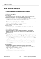
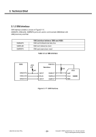
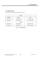
3. Technical Brief E. XGAM Subsystem The XGAM subsystem is a graphics acceleration module that provides hardware support in the creation of visual imagery and the transfer of this data to a display. The XGAM also provides support for connecting a Camera module. The visual data could be graphics, still images, or video. The XGAM subsystem is handled and provided by Ericsson. F. System Control Subsystem The SYSCON resides at the top level of the circuit architecture and is responsible for clock generation and clock and reset distribution within the digital baseband controller, as well as to external devices. The block is a slave peripheral under control of the ARM processor. The programming of the SYSCON controls the fundamental modes of operation within the digital baseband controller. Individual blocks can also be reset and their clocks held inactive by accessing the appropriate control registers. 3.1.4 RF Interface A. Asta Interface Asta controls GSM RF part using these signals through GSM RF chip-Gimli. • RF_DATA_A • RF_DATA_B • RF_DATA_C • RF_DATA_STRB Figure 3-1- 5. Schematic of Asta RF Interface B. WCDMA Radio Link Interface • RF_WCDMA_PA_0_EN • RF_WCDMA_PA_1_EN • RF_WCDMA_DCDC_EN • RF_WCDMA_PWRDET_EN Y4 RF_DATA_A AA2 RF_DATA_B Y3 RF_DATA_C Y2 RF_DATA_STRB QDATA_AMP_MSB IDATA_FREQ_MSB AMP_LSB_FREQ_LSB DCLK_DATSTR WPA0_EN TP300 WDCDC_EN WPOW_DET_EN WRX_I_N WRX_I_P WRX_Q_N WRX_Q_P WTX_I_N WTX_I_P WTX_Q_N WTX_Q_P WPOW_DET AB8 RF_WCDMA_PA_0_EN V7 RF_WCDMA_PA_1_EN AB5 RF_WCDMA_DCDC_EN AB6 RF_WCDMA_PWRDET_EN Y10 ADC_I_NEG W10 ADC_I_POS W9 ADC_Q_NEG Y9 ADC_Q_POS Y8 DAC_I_NEG W8 DAC_I_POS W7 DAC_Q_NEG Y7 DAC_Q_POS AB7 TX_POW Copyright © 2007 LG Electronics. Inc. All right reserved. Only for training and service purposes Figure 3-1-6. Schematic of WCDMA RF Interface - 25 - LGE Internal Use Only
-
 1
1 -
2
-
3
-
4
-
5
-
6
-
7
-
8
-
9
-
10
-
11
-
12
-
13
-
14
-
15
-
16
-
17
-
18
-
 19
19 -
 20
20 -
 21
21 -
 22
22 -
 23
23 -
 24
24 -
 25
25 -
 26
26 -
 27
27 -
 28
28 -
 29
29 -
30
-
31
-
32
-
33
-
34
-
35
-
36
-
37
-
38
-
39
-
40
-
41
-
42
-
43
-
44
-
45
-
46
-
47
-
48
-
49
-
50
-
51
-
52
-
53
-
54
-
55
-
56
-
57
-
58
-
59
-
60
-
61
-
62
-
63
-
64
-
65
-
66
-
67
-
68
-
69
-
70
-
71
-
72
-
73
-
74
-
75
-
76
-
77
-
78
-
79
-
80
-
81
-
82
-
83
-
84
-
85
-
86
-
87
-
88
-
89
-
90
-
91
-
92
-
93
-
94
-
95
-
96
-
97
-
98
-
99
-
100
-
101
-
102
-
103
-
104
-
105
-
106
-
107
-
108
-
109
-
110
-
111
-
112
-
113
-
114
-
115
-
116
-
117
-
118
-
119
-
120
-
121
-
122
-
123
-
124
-
125
-
126
-
127
-
128
-
129
-
130
-
131
-
132
-
133
-
134
-
135
-
136
-
137
-
138
-
139
-
140
-
141
-
142
-
143
-
144
-
145
-
146
-
147
-
148
-
149
-
150
-
151
-
152
-
153
-
154
-
155
-
156
-
157
-
158
-
159
-
160
-
161
-
162
-
163
-
164
-
165
-
166
-
167
-
168
-
169
-
170
-
171
-
172
-
173
-
174
-
175
-
176
-
177
-
178
-
179
-
180
-
181
-
182
-
183
-
184
-
185
-
186
-
187
-
188
-
189
-
190
-
191
-
192
-
193
-
194
-
195
-
196
-
197
-
198
-
199
-
200
-
201
-
202
-
203
-
204
-
205
-
206
-
207
-
208
-
209
 |
 |
