LG KU580 Service Manual - Page 41
Block Description - software
 |
View all LG KU580 manuals
Add to My Manuals
Save this manual to your list of manuals |
Page 41 highlights
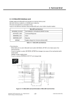
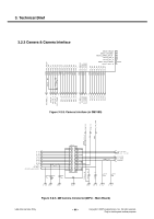
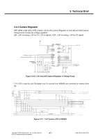
3. Technical Brief 3.2.2 Block Description A. GAM Controller(GAMCON) The GAM Controller (GAMCON) is responsible for clock gating and distribution within the GAM module. GAMCON receives the HCLK from SYSCON and distributes to GRAPHCON, GRAM, PDI and CDI. GAMCON also distributes the GAM reset signal to GRAPHCON, GRAM, PDI and CDI. The reset signals CIRES_N and PDIRES_N are distributed from GAMCON to the camera and display module respectively, see Figure 2.28. The CIPCLK is used to clock the received data into the camera data interface. The CIPCLK can be in the range of 100 kHz to 16 MHz. B. Graphics RAM (GRAM) Block GAM includes 160 kB of graphics memory (GRAM) in order to support display screen sizes of QCIF + alfa display size and three frame buffers when decoding QCIF video. The GRAM can be accessed in 8, 16 or 32-bit mode. Write access takes a single AHB clock cycle. Non-sequential read and the first access of a sequential read access takes two AHB clock cycles. Subsequent sequential read access take a single AHB clock cycle. The GRAM contains both frame buffer and temporary data. There are three image areas with one used for normal MMI graphics and the other two areas used for still images, video frames or camera frames. The three image areas can be combined into one frame buffer. GRAM is required to transfer a VGA (640 by 480 pixels) image from the camera data interface (CDI) over DMA at 100 MBit/s, within a 50 ms timeframe. The GRAM is used as a buffer, but the average transfer bandwidth required is approximately 3 Mword/s (32-bit word), that is 12 MByte/s. C. Graphics Controller (GRAPHCON) Block GRAPHCON is controlled by the application CPU and can perform operations on pixels and image areas. Images can be moved and merged with other images and text. The GRAPHCON block receives graphical objects from GRAM and performers the appropriate graphical manipulation. The resulting data is transfers to the display interface (PDI). GRAPHCON can receive images from the camera data interface (CDI) and send them to the PDI automatically. GRAPHCON performs conversion from YUV to RGB and can scale (zoom) still or video images. D. Programmable Display Interface (PDI) Block The programmable display interface (PDI) is designed to interface both parallel and serial display modules. The display data is transferred from the 32 word FIFO on GAMCON to the display module via the PDI block. The PDI block is built around a micro controller and executes 16-bit instruction words to individually control the I/O ports. It has a 128 byte program memory, programmable by the CPU, which can store up to 64 instructions. The CPU transfers all set-up and control data to the display. Data is transferred to PDI as 32-bit words, which in turn writes 8-bit data to the display. The programmable PDI block is configured at the software build stage, to support either parallel interface such as PPI or serial interface such as SSI or I2C. LGE Internal Use Only - 42 - Copyright © 2007 LG Electronics. Inc. All right reserved. Only for training and service purposes
-
 1
1 -
2
-
3
-
4
-
5
-
6
-
7
-
8
-
9
-
10
-
11
-
12
-
13
-
14
-
15
-
16
-
17
-
18
-
19
-
20
-
21
-
22
-
23
-
24
-
25
-
26
-
27
-
28
-
29
-
30
-
31
-
32
-
33
-
34
-
35
-
 36
36 -
 37
37 -
 38
38 -
 39
39 -
 40
40 -
 41
41 -
 42
42 -
 43
43 -
 44
44 -
 45
45 -
 46
46 -
47
-
48
-
49
-
50
-
51
-
52
-
53
-
54
-
55
-
56
-
57
-
58
-
59
-
60
-
61
-
62
-
63
-
64
-
65
-
66
-
67
-
68
-
69
-
70
-
71
-
72
-
73
-
74
-
75
-
76
-
77
-
78
-
79
-
80
-
81
-
82
-
83
-
84
-
85
-
86
-
87
-
88
-
89
-
90
-
91
-
92
-
93
-
94
-
95
-
96
-
97
-
98
-
99
-
100
-
101
-
102
-
103
-
104
-
105
-
106
-
107
-
108
-
109
-
110
-
111
-
112
-
113
-
114
-
115
-
116
-
117
-
118
-
119
-
120
-
121
-
122
-
123
-
124
-
125
-
126
-
127
-
128
-
129
-
130
-
131
-
132
-
133
-
134
-
135
-
136
-
137
-
138
-
139
-
140
-
141
-
142
-
143
-
144
-
145
-
146
-
147
-
148
-
149
-
150
-
151
-
152
-
153
-
154
-
155
-
156
-
157
-
158
-
159
-
160
-
161
-
162
-
163
-
164
-
165
-
166
-
167
-
168
-
169
-
170
-
171
-
172
-
173
-
174
-
175
-
176
-
177
-
178
-
179
-
180
-
181
-
182
-
183
-
184
-
185
-
186
-
187
-
188
-
189
-
190
-
191
-
192
-
193
-
194
-
195
-
196
-
197
-
198
-
199
-
200
-
201
-
202
-
203
-
204
-
205
-
206
-
207
-
208
-
209
 |
 |
