Lenovo PC 300PL Techical Information Manual - Page 33
Appendix A. Connector pin assignments, Monitor connector
 |
View all Lenovo PC 300PL manuals
Add to My Manuals
Save this manual to your list of manuals |
Page 33 highlights
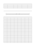
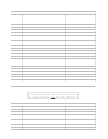
Appendix A. Connector pin assignments Appendix A. Connector pin assignments The following figures show the pin assignments for various system board connectors. Monitor connector 5 10 15 1 6 11 Figure 15. Monitor port connector pin assignments-SVGA Pin Signal I/O Pin 1 Red O 2 3 Blue O 4 5 Ground NA 6 7 Green ground NA 8 9 +5 V, used by DDC2B NA 10 11 Monitor ID 0 - Not I 12 used 13 Horizontal sync O 14 15 DDC2B clock I/O 1 C1 C2 Signal I/O Green O Monitor ID 2 - Not I used Red ground NA Blue ground NA Ground NA DDC2B serial data I/O Vertical sync O C3 C4 C5 Figure 16. Monitor port connector pin assignments-DVI main pin field Pin Signal I/O Pin Signal I/O 1 TMDS data 2+ O 2 TMDS data 2- O 3 TMDS data 2/4 return N/A 4 TMDS data 4-* O 5 TMDS data 4+* O 6 DDC clock I/O 7 DDC data I/O 8 Analog vertical sync O 9 TMDS data 1- O 10 TMDS data 1+ O 11 TMDS data 1/3 shield N/A 12 TMDS data 3+* O 13 TMDS data 3+* O 14 +5V power O 15 Ground N/A 16 Hot plug detect O 17 TMDS data 0- O 18 TMDS data 0+ O 19 Return N/A 20 TMDS D5* O 21 TMDS data 5+* O 22 TMDS clock shield N/A 23 TMDS clock+ O 24 TMDS clock- O © Copyright IBM Corp. September 1999 25
-
 1
1 -
2
-
3
-
4
-
5
-
6
-
7
-
8
-
9
-
10
-
11
-
12
-
13
-
14
-
15
-
16
-
17
-
18
-
19
-
20
-
21
-
22
-
23
-
24
-
25
-
26
-
27
-
 28
28 -
 29
29 -
 30
30 -
 31
31 -
 32
32 -
 33
33 -
 34
34 -
 35
35 -
 36
36 -
 37
37 -
 38
38 -
39
-
40
-
41
-
42
-
43
-
44
-
45
-
46
-
47
-
48
-
49
-
50
-
51
-
52
-
53
-
54
 |
 |
