Lenovo PC 300PL Techical Information Manual - Page 44
Appendix B. System address maps, System memory map, Input/output address map
 |
View all Lenovo PC 300PL manuals
Add to My Manuals
Save this manual to your list of manuals |
Page 44 highlights
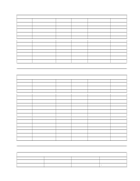
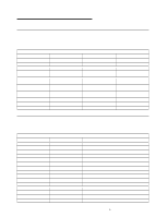
Appendix B. System address maps Appendix B. System address maps System memory map The first 640 KB of system board RAM is mapped starting at address hex 0000000. A 256 byte area and a 1 KB area of this RAM are reserved for BIOS data areas. Memory can be mapped differently if POST detects an error. Figure 35. System memory map Address range (decimal) Address range (hex) 0 K - 512 K 00000-7FFFF 512 K - 639 K 80000-9FBFF 639 K - 640 K 9FC00-9FFFF 640 K - 767 K A0000-BFFFF 768 K - 800 K C0000 to C7FFF 800 K - 896 K C8000-DFFFF 896 K - 1 MB E0000-FFFFF 1 MB - 16 MB 16 MB - 4095.872 MB 100000-FFFFFF 1000000-FFDFFFF FFFE0000 - FFFFFFFF Size 512 KB 127 KB 1 KB 128 KB 32 KB 96 KB 128 KB 15 MB 4079.8 MB 128 KB Description Conventional Extended conventional Extended BIOS data Dynamic video memory display cache Video ROM BIOS (shadowed) PCI space, available to adapter ROMs System ROM BIOS (main memory shadowed) PCI space PCI space (positive decode) System ROM BIOS Input/output address map The following figure lists resource assignments for the I/O address map. Any addresses that are not shown are reserved. Figure 36 (Page 1 of 3). I/O address map Address (Hex) Size 0000-000F 16 bytes 0010-001F 16 bytes 0020-0021 2 bytes 0022-003F 30 bytes 0040-0043 4 bytes 0044-00FF 28 bytes 0060 1 byte 0061 1 byte 0064 1 byte 0070, bit 7 1 bit 0070, bits 6:0 1 bit 0071 1 byte 0072-007F 14 bytes 0080 1 byte 008F 1 byte Description DMA 1 General I/O locations - available to PCI bus Interrupt controller 1 General I/0 locations - available to PCI bus Counter/timer 1 General I/0 locations - available to PCI bus Keyboard controller byte - reset IRQ PIIX4, system port B Keyboard controller, CMD/STAT byte Enable NMI Real-time clock, address Real-time clock, data General I/O locations - available to PCI bus POST checkpoint register during POST only Refresh page register 36 © Copyright IBM Corp. September 1999
-
 1
1 -
2
-
3
-
4
-
5
-
6
-
7
-
8
-
9
-
10
-
11
-
12
-
13
-
14
-
15
-
16
-
17
-
18
-
19
-
20
-
21
-
22
-
23
-
24
-
25
-
26
-
27
-
28
-
29
-
30
-
31
-
32
-
33
-
34
-
35
-
36
-
37
-
38
-
 39
39 -
 40
40 -
 41
41 -
 42
42 -
 43
43 -
 44
44 -
 45
45 -
 46
46 -
 47
47 -
 48
48 -
 49
49 -
50
-
51
-
52
-
53
-
54
 |
 |
