Lenovo PC 300PL Techical Information Manual - Page 45
of 3. I/O address map, SMC PC37C673, Serial port 3 or 4
 |
View all Lenovo PC 300PL manuals
Add to My Manuals
Save this manual to your list of manuals |
Page 45 highlights
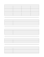
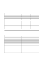
Figure 36 (Page 2 of 3). I/O address map Address (Hex) Size 0080-008F 16 bytes 0090-0091 15 bytes 0092 1 byte 0093-009F 15 bytes 00A0-00A1 2 bytes 00A2-00BF 30 bytes 00C0-00DF 31 bytes 00E0-00EF 16 bytes 00F0 1 byte 00F1-016F 127 bytes 0170-0177 8 bytes 01F0-01F7 8 bytes 0200-0207 8 bytes 0220-0227 8 bytes 0228-0277 80 bytes 0278-027F 8 bytes 0280-02E7 102 bytes 02E8-02EF 8 bytes 02F8-02FF 8 bytes 0338-033F 8 bytes 0340-036F 48 bytes 0370-0371. 2 bytes 0372-0375 4 bytes 0376-0377 2 bytes 0378-037F 8 bytes 0380-03B3 52 bytes 03B4-03B7 4 bytes 03BA 1 byte 03BC-03BE 16 bytes 03C0-03CF 16 bytes 03D4-03D7 4 bytes 03DA 1 byte 03D0-03DF 11 bytes 03E0-03E7 8 bytes 03E8-03EF 8 bytes 03F0-03F5 6 bytes 03F6 1 byte 03F7 (Write) 1 byte 03F7, bit 7 1 bit 03F7, bits 6:0 7 bits 03F8-03FF 8 bytes 0400-047F 128 bytes 0480-048F 16 bytes Appendix B. System address maps Description ICH1, DMA page registers General I/O locations - available to PCI bus PS/2 keyboard controller registers General I/O locations Interrupt controller 2 APM control DMA 2 General I/O locations - available to PCI bus BX, Coprocessor Error register General I/O locations - available to PCI bus Secondary IDE channel Primary IDE channel Available SMC 37C673, Serial port 3 or 4 General I/O locations - available to PCI bus SMC 27C673, LPT3 Available SMC PC37C673, Serial port 3 or 4 COM2 SMC PC37C673, serial port 3 or 4 Available SMC SIO system board Plug and Play index/data registers Available IDE channel 1 command LPT2 Available Video Video LPT1 Video Video Video Available Available COM3 or COM4 Diskette channel 1 Primary IDE channel command port Diskette channel 1 command Diskette disk change channel Primary IDE channel status port COM1 Available DMA channel high page registers Appendix B. System address maps 37
-
 1
1 -
2
-
3
-
4
-
5
-
6
-
7
-
8
-
9
-
10
-
11
-
12
-
13
-
14
-
15
-
16
-
17
-
18
-
19
-
20
-
21
-
22
-
23
-
24
-
25
-
26
-
27
-
28
-
29
-
30
-
31
-
32
-
33
-
34
-
35
-
36
-
37
-
38
-
39
-
 40
40 -
 41
41 -
 42
42 -
 43
43 -
 44
44 -
 45
45 -
 46
46 -
 47
47 -
 48
48 -
 49
49 -
 50
50 -
51
-
52
-
53
-
54
 |
 |
