Sharp XL-UH260 Service Manual - Page 96
Ic701 Vhim66005af-1:fl Driver, Pin Configuration, Pin Configuration Of Ic, Block
 |
View all Sharp XL-UH260 manuals
Add to My Manuals
Save this manual to your list of manuals |
Page 96 highlights
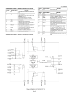
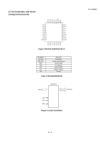
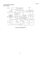
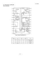
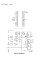
XL-UH260 IC701 VHIM66005AF-1:FL DRIVER PIN CONFIGURATION DIG11 1 DIG10 2 DIG09 3 DIG08 4 DIG07 5 Digit DIG06 6 outputs DIG05 7 DIG04 8 DIG03 9 DIG02 10 DIG01 11 DIG00 12 Reset input RESET 13 Chip select input CS 14 Shift clock input SCK 15 Serial data input SDATA 16 Universal bidirectional ports P1 17 P0 18 VCC1 19 Clock output XOUT 20 Clock input XIN 21 VSS 22 SEG35 23 SEG34 24 SEG33 25 SEG32 26 Segment outputs SEG31 27 SEG30 28 SEG29 29 SEG28 30 SEG27 31 Vp 32 64 DIG12/SEG36 63 DIG13/SEG37 62 DIG14/SEG38 61 DIG15/SEG39 60 VCC2 59 SEG00 Digit/ segment outputs 58 SEG01 57 SEG02 56 SEG03 55 SEG04 54 SEG05 53 SEG06 52 SEG07 51 SEG08 50 SEG09 49 SEG10 48 SEG11 47 46 SEG12 SEG13 Segment outputs 45 SEG14 44 SEG15 43 SEG16 42 SEG17 41 SEG18 40 SEG19 39 SEG20 38 SEG21 37 SEG22 36 SEG23 35 SEG24 34 SEG25 33 SEG26 Figure 8 PIN CONFIGURATION OF IC BLOCK DIAGRAM Display code RAM Bank 1 : 8bit x 16 Bank 2 : 8bit x 64 CGROM (35bit x 160) CS 14 SCK 15 SDATA 16 code write Serial data receive circuit Code/ command control circuit CGRAM dot data write (35bit x 16) code select XIN 21 XOUT 20 Clock generator timing clock Display controller scan pulse RESET 13 VCC1 19 VCC2 60 VSS 22 Vp 32 2 Figure 9 BLOCK DIAGRAM OF IC 8 - 8 Segment output circuit Segment/ Digit select/ output circuit 59 SEG00 33 SEG26 31 SEG27 24 SEG34 23 SEG35 64 DIG12/ SEG36 63 DIG13/ SEG37 62 DIG14/ SEG38 61 DIG15/ SEG39 Digit output circuit 12 DIG00 1 DIG11 18 P0 17 P1
-
 1
1 -
2
-
3
-
4
-
5
-
6
-
7
-
8
-
9
-
10
-
11
-
12
-
13
-
14
-
15
-
16
-
17
-
18
-
19
-
20
-
21
-
22
-
23
-
24
-
25
-
26
-
27
-
28
-
29
-
30
-
31
-
32
-
33
-
34
-
35
-
36
-
37
-
38
-
39
-
40
-
41
-
42
-
43
-
44
-
45
-
46
-
47
-
48
-
49
-
50
-
51
-
52
-
53
-
54
-
55
-
56
-
57
-
58
-
59
-
60
-
61
-
62
-
63
-
64
-
65
-
66
-
67
-
68
-
69
-
70
-
71
-
72
-
73
-
74
-
75
-
76
-
77
-
78
-
79
-
80
-
81
-
82
-
83
-
84
-
85
-
86
-
87
-
88
-
89
-
90
-
 91
91 -
 92
92 -
 93
93 -
 94
94 -
 95
95 -
 96
96 -
 97
97 -
 98
98 -
 99
99 -
 100
100 -
 101
101 -
102
-
103
-
104
-
105
-
106
-
107
-
108
-
109
-
110
-
111
-
112
-
113
-
114
-
115
-
116
-
117
-
118
-
119
-
120
-
121
-
122
-
123
-
124
 |
 |
