HP DL360 Memory technology evolution: an overview of system memory technologie - Page 20
commands and write data to the FB-DIMMs while the inbound links transmit read data back to
 |
UPC - 613326948835
View all HP DL360 manuals
Add to My Manuals
Save this manual to your list of manuals |
Page 20 highlights
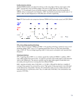
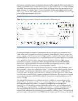
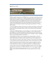
Each stub-bus connection creates an impedance discontinuity that negatively affects signal integrity. In addition, each DIMM creates an electrical load on the bus. The electrical load accumulates as DIMMs are added. These factors decrease the number DIMMs per channel that can be supported as the bus speed increases. For example, Figure 16 shows the number of loads supported per channel at data rates ranging from PC 100 to DDR-3 1600. Note that the number of supported loads drops from eight to two as data rates increase to DDR2 800. Figure 16. Maximum number of loads per channel based on DRAM data rate Increasing the number of channels to compensate for the drop in capacity per channel was not a viable option due to increased cost and board complexity. System designers had two options: limit memory capacity so that fewer errors occur at higher speeds, or use slower bus speeds and increase the DRAM density. For future generations of high-performance servers, neither option was acceptable. Future generations of servers require improved memory architecture to achieve higher memory bandwidth and capacity. Consequently, JEDEC developed the Fully-Buffered DIMM (FB-DIMM) specification, a serial interface that eliminates the parallel stub-bus topology and allows higher memory bandwidth while maintaining or increasing memory capacity. The FB-DIMM architecture has serial links between the memory controller and the FB-DIMMs, which are connected in a daisy chain configuration (Figure 17). Relative to the memory controller, there are ten outbound links and fourteen inbound links, also known as southbound and northbound links, respectively. These serial links connect the memory controller to an advanced memory buffer (AMB) chip that resides on each FB-DIMM, creating a point-to-point architecture. The outbound links transmit commands and write data to the FB-DIMMs while the inbound links transmit read data back to the memory controller. The clock signal is distributed over a different set of pins. In addition to communicating over the Outbound lanes, the memory controller communicates configuration information with each AMB over the System Management bus (SMBus). The AMB is an intelligent chip that manages serial communication with the memory controller and parallel communication with local DRAM devices. Each AMB receives signals (address, write data, and command information) through the outbound links and re-transmits the signal to the next FB-DIMM on the channel. Each AMB decodes the command data and ignores the commands that are targeted for a different DIMM. The targeted AMB performs a read or write operation to local DRAM devices through a parallel interface. In the case of 20
-
 1
1 -
2
-
3
-
4
-
5
-
6
-
7
-
8
-
9
-
10
-
11
-
12
-
13
-
14
-
 15
15 -
 16
16 -
 17
17 -
 18
18 -
 19
19 -
 20
20 -
 21
21 -
 22
22 -
 23
23 -
 24
24
 |
 |
