HP DL360 Memory technology evolution: an overview of system memory technologie - Page 22
clocks of additional delay. This delay cannot be avoided when using a very fast packet protocol.
 |
UPC - 613326948835
View all HP DL360 manuals
Add to My Manuals
Save this manual to your list of manuals |
Page 22 highlights
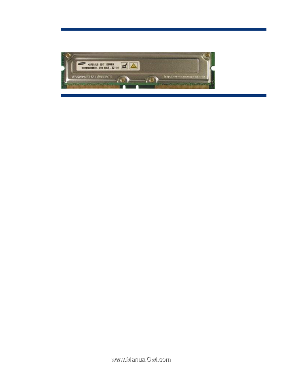
Figure 18. Rambus DRAM RDRAM is capable of supporting up to 32 RDRAM devices on one memory channel while maintaining a 1.2-GHz data rate. Through the use of a repeater chip, even more devices can be placed on one RDRAM channel. The repeater interfaces to two different RDRAM channels and passes the data and command signals between them. One channel communicates with the memory controller, and the other channel communicates with the RDRAM devices. Thus, the memory controller essentially communicates only with the repeater chips. Up to eight repeater chips can be placed on the memory controller, and 32 RDRAM devices can be placed on each channel. This allows one channel to support a maximum of 256 devices. However, using the repeater chips will add 1 to 1.5 clocks of additional delay. To account for differences in distance of the devices on the channel, more latency in increments of the clock can be added. This allows the memory controller to receive data from all devices in the same amount of time, thus preventing data collision on the bus when consecutive reads are performed to different devices. Another feature of RDRAM that helps to increase the efficiency is an internal 128-bit write buffer. All write data goes into this buffer before being sent to the DRAM core. The write buffer reduces the delay needed to turn around the internal data bus by allowing the sense amps to remain in the read direction until data needs to be retired from the buffer to the core. Essentially, a read can immediately follow a write with little bandwidth lost on the data bus. While the RDRAM bus efficiency is high, the packet protocol increases the latency. The packet translation between the internal memory controller bus and the fast external bus requires one to two clocks of additional delay. This delay cannot be avoided when using a very fast packet protocol. With the high data rate of Rambus, signal integrity is troublesome. System boards must be designed to accommodate the extremely stringent timing of Rambus, and this increases product time to market. Additionally, each Rambus channel is limited to 32 devices, imposing an upper limit on memory capacity supported by a single bus. Use of repeater chips enables use of additional devices and increases potential memory capacity, but repeater chips have been very challenging to design. Finally, the larger dies and more limited production of RDRAM compared to those of other memory technologies have increased the cost of RDRAM. RDRAM still costs up to twice as much as SDRAM. RDRAM technology offers performance advantages and lower pin count than SDRAM and DDR SDRAM. However, SDRAM and DDR SDRAM offer more memory capacity and lower cost than RDRAM. 22
-
 1
1 -
2
-
3
-
4
-
5
-
6
-
7
-
8
-
9
-
10
-
11
-
12
-
13
-
14
-
15
-
16
-
 17
17 -
 18
18 -
 19
19 -
 20
20 -
 21
21 -
 22
22 -
 23
23 -
 24
24
 |
 |