HP DL360 Memory technology evolution: an overview of system memory technologie - Page 21
Rambus DRAM
 |
UPC - 613326948835
View all HP DL360 manuals
Add to My Manuals
Save this manual to your list of manuals |
Page 21 highlights
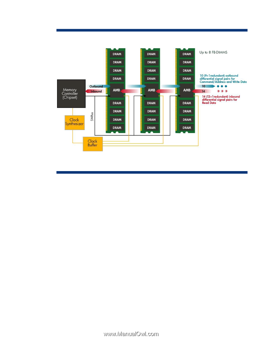
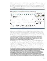
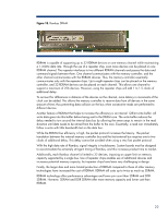
a read operation, the AMB serializes data from the DRAM devices and transmits it to the memory controller through the inbound links. Figure 17. Serial communication between daisy-chained FB-DIMMs on a single channel NOTE: AMD® Opteron® and Intel® Xeon® E55xx/X55xx CPU designs include the memory controller and clock functions integrated into processor module. When using DDR2-667 DRAM on the FB-DIMM, the peak theoretical throughput of the inbound links is 5.4 GB/s. The peak theoretical throughput of the outbound links is half that: approximately 2.6 GB/s. Rambus DRAM Rambus DRAM (RDRAM) allows data transfer through a bus operating in a higher frequency range than DDR SDRAM. In essence, Rambus moves small amounts of data very rapidly, whereas DDR SDRAM moves large amounts of data more slowly. The Rambus design consists of three key elements: RDRAMs, Rambus application-specific integrated circuits, and an interconnect called the Rambus Channel. The Rambus design provides higher performance than traditional SDRAM because RDRAM transfers data on both edges of a synchronous, high-speed clock pulse. RDRAM uses a separate row and column command bus that allows issuing multiple commands at the same time, thereby increasing the bandwidth efficiency of the memory bus. This dual command bus is a unique feature of RDRAM. With only an 8-bit-wide command bus and an 18-bit data bus, RDRAM (Figure 18) has the lowest signal count of all of the memory technologies. RDRAM incorporates a packet protocol and is capable of operating at 800 MHz and providing a peak bandwidth of 2.4 GB/s. One packet of information is transferred in 8 ticks of the clock, which allows sending128 bits of data in a 150-MHz clock period. Since it requires 8 ticks of the clock to transfer a packet, the internal memory controller only needs to run at a speed of 150 MHz to keep up with the packet transfer rate at 1.2 GHz. This allows for plenty of timing margin in the design of the memory controller. 21
-
 1
1 -
2
-
3
-
4
-
5
-
6
-
7
-
8
-
9
-
10
-
11
-
12
-
13
-
14
-
15
-
 16
16 -
 17
17 -
 18
18 -
 19
19 -
 20
20 -
 21
21 -
 22
22 -
 23
23 -
 24
24
 |
 |