HP DL360 Memory technology evolution: an overview of system memory technologie - Page 8
Registered SDRAM modules, DIMM configurations
 |
UPC - 613326948835
View all HP DL360 manuals
Add to My Manuals
Save this manual to your list of manuals |
Page 8 highlights
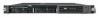
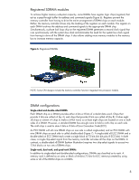
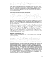
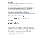
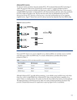
Registered SDRAM modules To achieve higher memory subsystem capacity, some DIMMs have register logic chips (registers) that act as a pass-through buffer for address and command signals (Figure 6). Registers prevent the memory controller from having to drive the entire arrangement of DRAM chips on each module. Rather, the memory controller drives only the loading of the registers on each module. The register on each DIMM re-drives the address and command signals to the appropriate DRAM chip. Simultaneously, a phase lock loop chip on the registered DIMM generates a second clock signal that runs synchronously with the system bus clock and eliminates the need for the system bus clock signal from having to drive all the DRAM chips. It also allows adding more memory modules to the memory bus to increase memory capacity. Figure 6. Registered DIMMs NOTE: Some CPU designs include the memory controller function integrated into processor module. DIMM configurations Single-sided and double-sided DIMMs Each DRAM chip on a DIMM provides either 4 bits or 8 bits of a 64-bit data word. Chips that provide 4 bits are called x4 (by 4), and chips that provide 8 bits are called x8 (by 8). It takes eight x8 chips or sixteen x4 chips to make a 64-bit word, so at least eight chips are located on one or both sides of a DIMM. However, a standard DIMM has enough room to hold a ninth chip on each side. The ninth chip is used to store 4 bits or 8 bits of Error Correction Code (ECC). An ECC DIMM with all nine DRAM chips on one side is called single-sided, and an ECC DIMM with nine DRAM chips on each side is called double-sided (Figure 7). A single-sided x8 ECC DIMM and a double-sided x4 ECC DIMM each create a single block of 72 bits (64 bits plus 8 ECC bits). In both cases, a single chip-select signal from the memory controller activates all the chips on the DIMM. In contrast, a double-sided x8 DIMM (bottom illustration) requires two chip-select signals to access two 72-bit blocks on two sets of DRAM chips. Single-rank, dual-rank, and quad-rank DIMMs In addition to single-sided and double-sided configurations, DIMMs are classified as to rank. A memory rank is defined as an area or block of 64-bits (72 bits for ECC memory) created by using some or all of the DRAM chips on a DIMM. 8
-
 1
1 -
2
-
 3
3 -
 4
4 -
 5
5 -
 6
6 -
 7
7 -
 8
8 -
 9
9 -
 10
10 -
 11
11 -
 12
12 -
 13
13 -
14
-
15
-
16
-
17
-
18
-
19
-
20
-
21
-
22
-
23
-
24
 |
 |