HP DL360 Memory technology evolution: an overview of system memory technologie - Page 7
SDRAM technology
 |
UPC - 613326948835
View all HP DL360 manuals
Add to My Manuals
Save this manual to your list of manuals |
Page 7 highlights
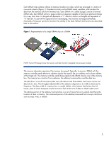
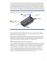
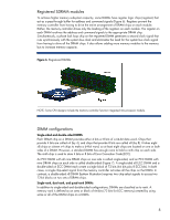
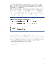
SDRAM technology FPM and EDO DRAMs are controlled asynchronously, that is, without a memory bus clock. The memory controller determines when to assert signals and when to expect data based on absolute timing. The inefficiencies of transferring data between a synchronous system bus and an asynchronous memory bus results in longer latency. Consequently, JEDEC-the electronics industry standards agency for memory devices and modules- developed the synchronous DRAM standard to reduce the number of system clock cycles required to read or write data. SDRAM uses a memory bus clock to synchronize the input and output signals on the memory chip. This simplifies the memory controller and reduces the latency from CPU to memory. In addition to synchronous operation and burst mode access, SDRAM has other features that accelerate data retrieval and increase memory capacity: multiple memory banks, greater bandwidth, and register logic chips. Figure 5 shows SDRAM DIMMs with two key notches that prevent incorrect installation and indicate the type of DRAM module. Figure 5. SDRAM DIMM with two notches Bank interleaving SDRAM divides memory into two to four banks for simultaneous access to more data. This division and simultaneous access is known as interleaving. Using a notebook analogy, two-way interleaving is like dividing each page in a notebook into two parts and having two assistants to each retrieve a different part of the page. Even though each assistant must take a break (be refreshed), breaks are staggered so that at least one assistant is working at all times. Therefore, they retrieve the data much faster than a single assistant could get the same data from one whole page, especially since no data can be accessed when a single assistant takes a break. In other words, while one memory bank is being accessed, the other bank remains ready to be accessed. This allows the processor to initiate a new memory access before the previous access completes and results in continuous data flow. Increased bandwidth The bandwidth capacity of the memory bus increases with its width (in bits) and its frequency (in MHz). By transferring 8 bytes (64 bits) at a time and running at 100 MHz, SDRAM increases memory bandwidth to 800 MB/s, 50 percent more than EDO DRAMs (533 MB/s at 66 MHz). 7
-
 1
1 -
 2
2 -
 3
3 -
 4
4 -
 5
5 -
 6
6 -
 7
7 -
 8
8 -
 9
9 -
 10
10 -
 11
11 -
 12
12 -
13
-
14
-
15
-
16
-
17
-
18
-
19
-
20
-
21
-
22
-
23
-
24
 |
 |
