HP DL360 Memory technology evolution: an overview of system memory technologie - Page 5
Memory access time, System bus timing
 |
UPC - 613326948835
View all HP DL360 manuals
Add to My Manuals
Save this manual to your list of manuals |
Page 5 highlights
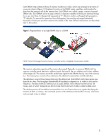
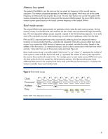
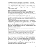
Memory access time The length of time it takes for DRAM to produce the data, from the CAS signal until the data is available on the data bus, is called the memory access time or CAS Latency. For asynchronous DRAM, memory access time is measured in billionths of a second (nanoseconds, ns). For synchronous DRAM, the memory access time is measured by the number of memory bus clocks. System bus timing A system bus clock controls all computer components that execute instructions or transfer data. Typically, the system chipset controls the speed, or frequency, of the system bus clock and thus regulates the traffic between the processor, main memory, PCI bus, and other peripheral buses. The bus clock is an electronic signal that alternates between two voltages (designated as "0" and "1" in Figure 3) at a specific frequency. The bus frequency is measured in millions of cycles per second, or megahertz (MHz). During each clock cycle, the voltage signal transitions from "0" to "1" and back to "0." A complete clock cycle is measured from one rising edge to the next rising edge. Data transfer along the memory bus can be triggered on either the rising edge or falling edge of the clock signal. Figure 3. Representation of a bus clock signal Over time, some computer components have gained in speed more than others have. For this reason, the components in a typical server are controlled by different clocks that run at different, but related, speeds. These clocks are created by using various clock multiplier and divider circuits to generate multiple signals based on the main system bus clock. For example, if the main system bus operates at 100 MHz, a divider circuit can generate a PCI bus frequency of 33 MHz (system clock ÷ 3) and a multiplier circuit can generate a processor frequency of 400 MHz (system clock x 4). Computer components that operate in whole multiples of the system clock are termed synchronous because they are "in sync" with the system clock. Synchronous components operate more efficiently than components that are not synchronized (asynchronous) with the system bus clock. With asynchronous components, either the rest of the system or the component itself must wait one or more additional clock cycles for data or instructions due to clock resynchronization. In contrast, synchronized components know on which clock cycle data will be available, thus eliminating these timing delays. 5
-
 1
1 -
 2
2 -
 3
3 -
 4
4 -
 5
5 -
 6
6 -
 7
7 -
 8
8 -
 9
9 -
 10
10 -
 11
11 -
12
-
13
-
14
-
15
-
16
-
17
-
18
-
19
-
20
-
21
-
22
-
23
-
24
 |
 |
