HP ProLiant BL660c Electrical signal integrity considerations for HP BladeSyst - Page 13
to a trace, see Test pads should not be used.
 |
View all HP ProLiant BL660c manuals
Add to My Manuals
Save this manual to your list of manuals |
Page 13 highlights
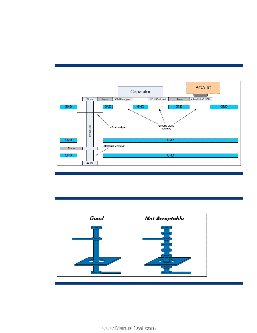
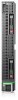
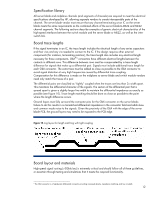
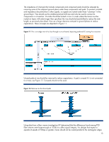
The impedance of channels that include components and component pads should be adjusted by removing some of the adjacent ground plane under these components and pads. To prevent crosstalk and impedance discontinuities in other signals, no signals are routed under these "cutaways" in the ground layer. Vias should use the smallest practical drill size and only be used to connect to components or connectors. Via stubs should be limited in size. In cases where the traces must be routed on layers with stubs longer than specified, the vias should be back-drilled to reduce the stub length, as previously described. Vias use a large clearance anti-pad in ground planes to reduce capacitance. These concepts are depicted in Figure 11. Figure 11. This is an edge view of a slice through a circuit board, depicting preferred IC routing for a receiver. Unused pads at vias should be removed to reduce capacitance. A pad is unused if it is not connected to a trace, see Figure 12. Test pads should not be used. Figure 12. Remove non-functional pads Using data from a fiber weave investigation HP determined that the differences found among PCB fiber weaves were large enough at 10Gb/s to affect signal integrity. For designs that expect to operate at speeds of 5Gbps or greater, traces should not be routed parallel to the rectangular edges 13
-
 1
1 -
2
-
3
-
4
-
5
-
6
-
7
-
 8
8 -
 9
9 -
 10
10 -
 11
11 -
 12
12 -
 13
13 -
 14
14 -
 15
15 -
 16
16
 |
 |