HP ProLiant BL660c Electrical signal integrity considerations for HP BladeSyst - Page 7
Stubs
 |
View all HP ProLiant BL660c manuals
Add to My Manuals
Save this manual to your list of manuals |
Page 7 highlights
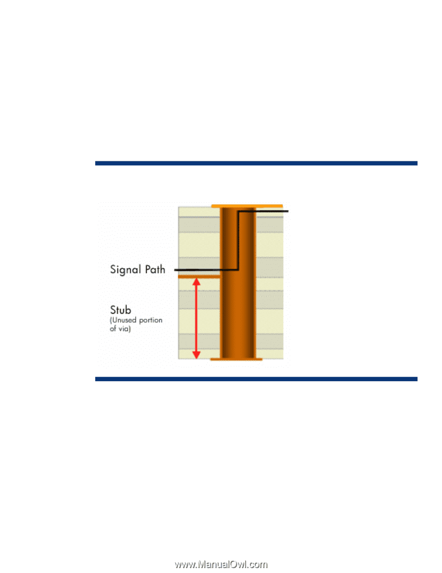
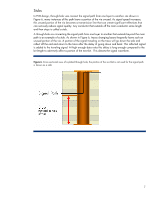
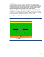
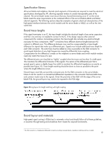
Stubs In PCB design, through-hole vias connect the signal path from one layer to another. As shown in Figure 6, many instances of this path leave a portion of the via unused. As signal speed increases, this unused portion of the via becomes a transmission line that can create significant reflections that can seriously reduce signal quality. Any conductor that extends off the main conductor some length and then stops is called a stub. A through-hole via connecting the signal path from one layer to another that extends beyond the main path is an example of a stub. As shown in Figure 6, traces changing layers frequently leave such an unused portion of the via. A portion of the signal traveling on the trace will go down the stub and reflect off the end and return to the trace after the delay of going down and back. This reflected signal is added to the traveling signal. At high enough data rates this delay is long enough compared to the bit length to adversely affect a portion of the next bit. This distorts the signal waveform. Figure 6. Cross sectional view of a plated through hole, the portion of the via that is not used for the signal path is known as a stub 7
-
 1
1 -
 2
2 -
 3
3 -
 4
4 -
 5
5 -
 6
6 -
 7
7 -
 8
8 -
 9
9 -
 10
10 -
 11
11 -
 12
12 -
13
-
14
-
15
-
16
 |
 |