Asus PSCH-SR SATA PSCH-SR User Manual English Version - Page 74
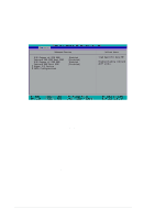
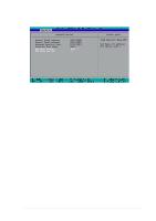
DRAM RAS# Precharge [3], Memory Parity Check [Enabled], System BIOS Cacheable [Enabled], Video BIOS
 |
View all Asus PSCH-SR SATA manuals
Add to My Manuals
Save this manual to your list of manuals |
Page 74 highlights
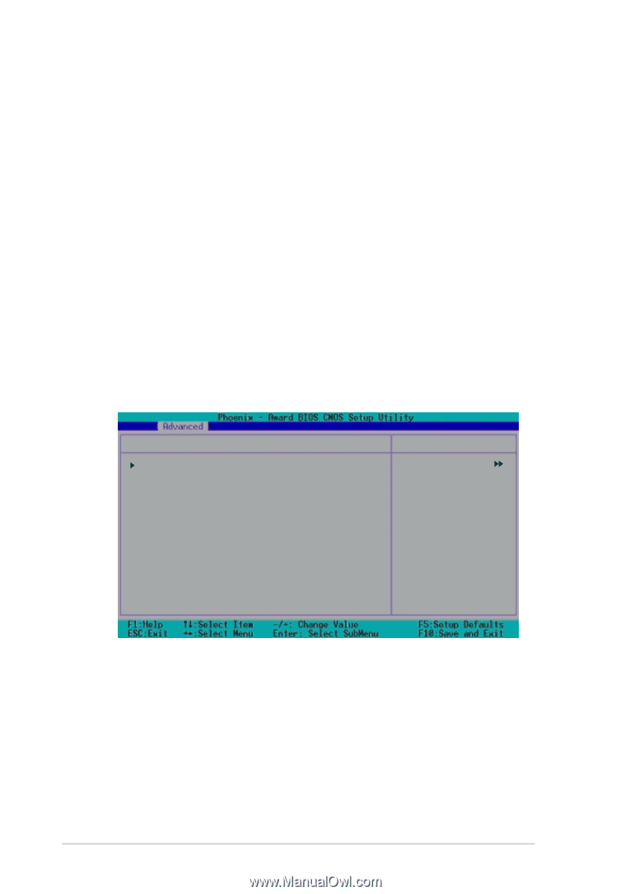
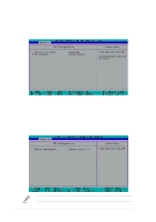
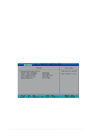
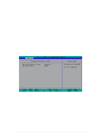
DRAM RAS# to CAS# Delay [3] Controls the latency between the DRAM active command and the read/ write command. Configuration options: [4] [3] [2] DRAM RAS# Precharge [3] This item controls the idle clocks after issuing a precharge command to the DDR SDRAM. Configuration options: [4] [3] [2] Memory Parity Check [Enabled] Allows memory parity checking option. This item is not user-configurable and set to [Enabled] by default. 4.4.4 Chipset This menu shows the chipset configuration settings. Select an item then press to display a sub-menu with additional items, or show a popup menu with the configuration options. Chipset Frequency/Voltage Control System BIOS Cacheable Video BIOS Cacheable Init Display First Auto Detect PCI Clk Spread Spectrum [Enabled] [Disabled] [PCI VGA Card] [Enabled] [+/- 0.35%] Select Menu Item Specific Help Press to set. System BIOS Cacheable [Enabled] Allows you to enable or disable the cache function of the system BIOS. Configuration options: [Disabled] [Enabled] Video BIOS Cacheable [Disabled] Allows you to enable or disable the cache function of the video BIOS. Setting to [Enabled] improves the display speed by caching the display data. Configuration options: [Disabled] [Enabled] 4-18 Chapter 4: BIOS Setup
-
 1
1 -
2
-
3
-
4
-
5
-
6
-
7
-
8
-
9
-
10
-
11
-
12
-
13
-
14
-
15
-
16
-
17
-
18
-
19
-
20
-
21
-
22
-
23
-
24
-
25
-
26
-
27
-
28
-
29
-
30
-
31
-
32
-
33
-
34
-
35
-
36
-
37
-
38
-
39
-
40
-
41
-
42
-
43
-
44
-
45
-
46
-
47
-
48
-
49
-
50
-
51
-
52
-
53
-
54
-
55
-
56
-
57
-
58
-
59
-
60
-
61
-
62
-
63
-
64
-
65
-
66
-
67
-
68
-
 69
69 -
 70
70 -
 71
71 -
 72
72 -
 73
73 -
 74
74 -
 75
75 -
 76
76 -
 77
77 -
 78
78 -
 79
79 -
80
-
81
-
82
-
83
-
84
-
85
-
86
-
87
-
88
-
89
-
90
-
91
-
92
-
93
-
94
-
95
-
96
-
97
-
98
-
99
-
100
-
101
-
102
 |
 |