Brother International HL 760 Service Manual - Page 11
Block, Diagram, shows, block, diagram
 |
UPC - 012502562832
View all Brother International HL 760 manuals
Add to My Manuals
Save this manual to your list of manuals |
Page 11 highlights
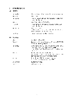
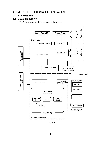
1.2 Main PCB Block Diagram Fig. 2.2 shows a block diagram of the main PCB. Reset Circuit CPU Core (R3041) BUS INT Program + Font ROM .IIII IIPPW 4 Mbytes rill RAM (1.0 Mbytes) Option RAM (SIMM) oil (max.32 Mbytes) rill Option Serial I/O 4 (RS232C & RS422A) ASIC Oscillator (4MHz) Address Decoder DRAM Control Timer FIFO DATA EXTENSION CDCC Parallel I/O --4-0-- To PC Soft Support EEPROM (512 x8 bits) EEPROM I/O Motor Driver 11 To Panel Sensor PCB Fig. 2.2 Pr Engine Control I/O II - 2
-
 1
1 -
2
-
3
-
4
-
5
-
 6
6 -
 7
7 -
 8
8 -
 9
9 -
 10
10 -
 11
11 -
 12
12 -
 13
13 -
 14
14 -
 15
15 -
 16
16 -
17
-
18
-
19
-
20
-
21
-
22
-
23
-
24
-
25
-
26
-
27
-
28
-
29
-
30
-
31
-
32
-
33
-
34
-
35
-
36
-
37
-
38
-
39
-
40
-
41
-
42
-
43
-
44
 |
 |

1.2
Main
PCB
Block
Diagram
Fig.
2.2
shows
a
block
diagram
of
the
main
PCB.
ASIC
Reset
Circuit
Program
+
Font
ROM
4
Mbytes
RAM
(1.0
Mbytes)
Option
RAM
(SIMM)
(max.32
Mbytes)
Option
Serial
I/O
(RS232C
&
RS422A)
CPU
Core
(R3041)
BUS
INT
.IIII
IIPPW
rill
Oscillator
(4MHz)
oil
rill
4
Address
Decoder
DRAM
Control
Timer
EEPROM
(512
x8
bits)
FIFO
DATA
EXTENSION
CDCC
Parallel
I/O
Soft
Support
Motor
Driver
11
To
Panel
Sensor
PCB
Fig.
2.2
Pr
EEPROM
I/O
Engine
Control
I/O
--4-0--
To
PC
I I
-
2