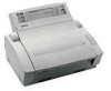
Brother International HL 760 Service Manual - Page 5
Disassembly, Reassembly, Troubleshooting, Appendices
 |
UPC - 012502562832
View all Brother International HL 760 manuals
Add to My Manuals
Save this manual to your list of manuals |
Page 5 highlights
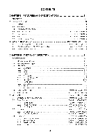
2.4.5 Cleaner Roller 2.4.6 Erase lamp 2.5 Print Process 2.5.1 2.5.2 2.5.3 2.5.4 2.5.5 2.5.6 Charging Exposure stage Developing Transfer Drum Cleaning Stage Erasing Stage CHAPTER III DISASSEMBLY AND REASSEMBLY 1. SAFETY PRECAUTIONS 2. DISASSEMBLING FLOW 3. DISASSEMBLING PROCEDURE 3.1 3.2 3.3 3.4 3.5 3.6 3.7 3.8 3.9 3.10 3.11 3.12 3.13 3.14 3.15 3.16 3.17 Drum Unit Top Cover Multi-purpose Paper Tray Assy Fixing Unit Scanner Unit Main PCB Assy Base Plate Assy Panel sensor PCB Assy Low-voltage Power Supply PCB Assy High-voltage Power Supply PCB Assy Fan Motor Drive Unit Main Motor Assy and Motor Heat Sink Gears and Solenoid Tray Extension Paper Eject Tray Assy Core 4. PACKING CHAPTER IV TROUBLESHOOTING 1. INTRODUCTION 1.1 Initial Check 1.2 Basic Procedure 2. IMAGE DEFECTS 2.1 Image Defect Examples 2.2 Troubleshooting Image Defects 3. TROUBLESHOOTING OF MALFUNCTIONS 4. INSPECTION MODE 4.1 Incorporated Inspection Modes 4.2 Error codes APPENDICES 1. Connection Diagram 2. Main PCB Circuit Diagram (1/3) 3. Main PCB Circuit Diagram (2/3) 4. Main PCB Circuit Diagram (3/3) 5. Panel/Sensor PCB Circuit Diagram 6. Low-Voltage Power Supply PCB Circuit Diagram 230V 7. Low-Voltage Power Supply PCB Circuit Diagram 115V 8. High-Voltage Power Supply PCB Circuit Diagram - - Refer to HL-730 (P I I-28) Refer to HL-730 (P 11-28) Refer to HL-730 (P 11-28) Refer to HL-730 (P.11-28) Refer to HL-730 (P. 11-29) Refer to HL-730 (P 11-30) Refer to HL-730 (P 11-30) Refer to HL-730 (P 11-31) Refer to HL-730 (P 11-31) III-1 III-1 III-2 III-3 I I I-3 I I I-3 I I I-4 II I-5 I I I-5 I I I-6 I I I-6 I I I-7 I I I-7 I I I-8 I I I-8 I I I-9 I II-9 II I-10 I I I-11 I I I-11 I I I-12 III-13 IV-1 Refer to HL-730 (PIV-1) Refer to HL-730 (P IV-1) Refer to HL-730 (P IV-2) Refer to HL-730 (P.IV-3) Refer to HL-730 (PIV-3) Refer to HL-730 (PIV-4) Refer to HL-730 (P.IV-12) IV-1 IV-1 IV-3 V-1 V-1 V-2 V-3 V-4 Refer to HL-730 (PV-6) V-5 V-6 Refer to HL-730 (PV-9)
-
 1
1 -
 2
2 -
 3
3 -
 4
4 -
 5
5 -
 6
6 -
 7
7 -
 8
8 -
 9
9 -
 10
10 -
 11
11 -
12
-
13
-
14
-
15
-
16
-
17
-
18
-
19
-
20
-
21
-
22
-
23
-
24
-
25
-
26
-
27
-
28
-
29
-
30
-
31
-
32
-
33
-
34
-
35
-
36
-
37
-
38
-
39
-
40
-
41
-
42
-
43
-
44
 |
 |
