Icom IC-R9500 Service Manual - Page 13
Logic Unit, Power Supply Circuits, Reg And Dcdc Units, Front Unit
 |
View all Icom IC-R9500 manuals
Add to My Manuals
Save this manual to your list of manuals |
Page 13 highlights
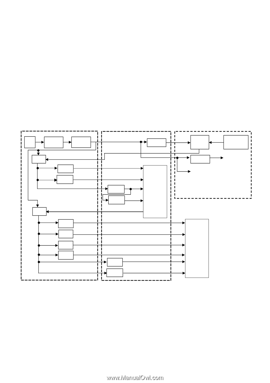
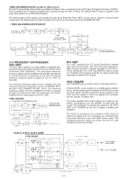
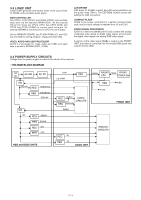
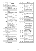
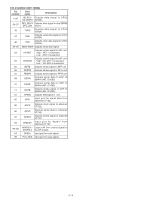
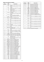
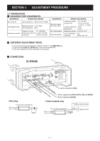
3-3 LOGIC UNIT LOGIC UNIT generally controls the whole of the circuit of the IC-R9500, and processes audio signal. MAIN CONTROLLER Two CPU's; IC103 (CPU1) and IC604 (CPU2) communicate each other via the dual port SRAM (IC51). As the external I/O port for these two CPU's, CPU1 has CPLD (IC52) and CPU2 has CPLD (IC605) to control each in/output. An external SDRAM is connected to the CPU1 for work space. On the MEMORY BOARD, two FLASH ROMs (IC1 and IC2) are mounted for storing program, image and audio files. VIDEO, AUDIO AND USB PROCESSOR IC203 is a processor for video, audio and USB, and each data is stored in SDRAM (IC201, IC202). LAN DRIVER LAN driver IC (IC404) conduct the LAN communications via the pulse trans (T401). The EEPROM (IC403) stores the settings for LAN connection. COMPACT FLASH IC402 is the power controller for inserted compact flash card, and its output voltage is selected from 5V and 3.3V. VIDEO SIGNAL PROCESSOR IC856 is a video encode/decode IC and converts the analog composite video signal to digital video signal, and converts the digital video signal into analog RGB video signal. A portion of the video signal (RGB) is output to the FRONT UNIT, and other is converted into the analog RGB signal and output from the J803. 3-4 POWER SUPPLY CIRCUITS Voltage from the power supply is routed to the whole of the receiver. • VOLTAGE BLOCK DIAGRAM AC AC-SW AC-DC IN SW VDD15V REG VDD3R3VA REG VDD3R3VB VDD15V SW 15V REG 3R3VA REG 3R3VB REG 28V REG -12V REG and DCDC UNITS H15V LG_PWR REG H3R3V FRONT PWRK FRONT CPU POWER SW REG H15V H5V REG REG VDD5V LOGIC CIRCUITS VDD1R2V PWRS FRONT UNIT REG 8V REG 5V LOGIC UNIT ANALOG CIRCUITS 3 - 5
-
 1
1 -
2
-
3
-
4
-
5
-
6
-
7
-
 8
8 -
 9
9 -
 10
10 -
 11
11 -
 12
12 -
 13
13 -
 14
14 -
 15
15 -
 16
16 -
 17
17 -
 18
18 -
19
-
20
-
21
-
22
-
23
-
24
-
25
-
26
-
27
-
28
-
29
-
30
-
31
-
32
-
33
-
34
-
35
-
36
-
37
-
38
-
39
-
40
-
41
-
42
-
43
-
44
-
45
-
46
-
47
-
48
-
49
-
50
-
51
-
52
-
53
-
54
-
55
-
56
-
57
-
58
-
59
-
60
-
61
-
62
-
63
-
64
-
65
-
66
-
67
-
68
-
69
-
70
-
71
-
72
-
73
-
74
-
75
-
76
-
77
-
78
-
79
-
80
-
81
-
82
-
83
-
84
-
85
-
86
-
87
-
88
-
89
-
90
-
91
-
92
-
93
-
94
-
95
-
96
-
97
-
98
-
99
-
100
-
101
-
102
-
103
-
104
-
105
-
106
-
107
-
108
-
109
-
110
-
111
-
112
-
113
-
114
-
115
-
116
-
117
-
118
-
119
-
120
-
121
-
122
-
123
-
124
-
125
-
126
-
127
-
128
-
129
-
130
-
131
-
132
-
133
-
134
-
135
-
136
-
137
-
138
 |
 |