Icom IC-R9500 Service Manual - Page 16
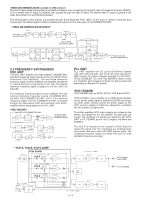
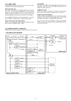
CPLD LOGIC UNIT; IC605, High : V/U ANT 1 is selected.
 |
View all Icom IC-R9500 manuals
Add to My Manuals
Save this manual to your list of manuals |
Page 16 highlights
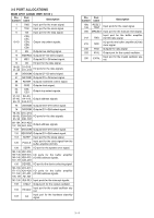
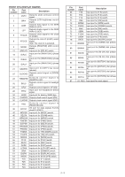
CPLD (LOGIC UNIT; IC605) Pin number Port name Description 1−27 H8_A13− Outputs data signal to CPU2 H8_WAIT# (IC604). 28−37 DPL_BUSY Outputs data signal to dual SRAM DPL_LB# (IC51). 45 TDO0 Outputs data signal to CPU2 (IC604). 47 TMS Outputs serial data signal to CPU2 (IC604). 48 TCK Outputs clock data signal to CPU2 (IC604). 49−58 IMS0−IMS7 Outputs serial data signal. Outputs control signal to ANT unit. 63 HFANTI High : ANT 1 is selected. Low : ANT 2 is selected. Outputs control signal to ANT unit. 64 HFANTO High : V/U ANT 1 is selected. Low : V/U ANT 2 is selected. 65 BSTB Outputs strobe signal to BPF unit. 66 RASTB Outputs strobe signal to RF-A unit. 67 RBSTB Outputs strobe signal to RF-B unit. 68 DSON Outputs serial data to DSP IC (MAIN UNIT; IC1005). 70 DSAP Outputs serial data to DSP IC (MAIN UNIT; IC1005). 71 DSTB Outputs strobe signal to DSP IC (MAIN UNIT; IC1005). 81 APIRQ Outputs IRQ signal to unit. 82 APSI Input port for serial data from attached UT-122. 85 APCK Outputs clock signal to attached UT-122. 86 APSO Outputs serial data to attached UT-122. 87 APSTB Outputs strobe signal to attached UT-122. 89 APBUSY Input port for "BUSY" from attached UT-122. 90−92 APAFSL1− Output AF line control signal to APAFSL3 the AF circuits. 94 DRESL Input port for reset signal. 99 PLD_RES Input port for reset signal. 3 - 8
-
 1
1 -
2
-
3
-
4
-
5
-
6
-
7
-
8
-
9
-
10
-
 11
11 -
 12
12 -
 13
13 -
 14
14 -
 15
15 -
 16
16 -
 17
17 -
 18
18 -
 19
19 -
 20
20 -
 21
21 -
22
-
23
-
24
-
25
-
26
-
27
-
28
-
29
-
30
-
31
-
32
-
33
-
34
-
35
-
36
-
37
-
38
-
39
-
40
-
41
-
42
-
43
-
44
-
45
-
46
-
47
-
48
-
49
-
50
-
51
-
52
-
53
-
54
-
55
-
56
-
57
-
58
-
59
-
60
-
61
-
62
-
63
-
64
-
65
-
66
-
67
-
68
-
69
-
70
-
71
-
72
-
73
-
74
-
75
-
76
-
77
-
78
-
79
-
80
-
81
-
82
-
83
-
84
-
85
-
86
-
87
-
88
-
89
-
90
-
91
-
92
-
93
-
94
-
95
-
96
-
97
-
98
-
99
-
100
-
101
-
102
-
103
-
104
-
105
-
106
-
107
-
108
-
109
-
110
-
111
-
112
-
113
-
114
-
115
-
116
-
117
-
118
-
119
-
120
-
121
-
122
-
123
-
124
-
125
-
126
-
127
-
128
-
129
-
130
-
131
-
132
-
133
-
134
-
135
-
136
-
137
-
138
 |
 |