Icom IC-R9500 Service Manual - Page 15
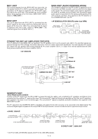
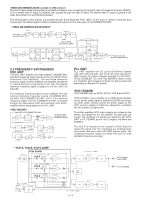
Main Cpu2 Logic Unit; Ic604, Dds Ic On The Scope/tv Unit.
 |
View all Icom IC-R9500 manuals
Add to My Manuals
Save this manual to your list of manuals |
Page 15 highlights
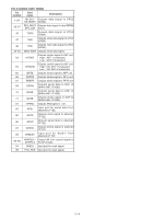
MAIN CPU2 (LOGIC UNIT; IC604) Pin Port number name Description 5-9 H8_A0-A4, 11-17 H8_A5-A11, Output address bus signals. 19, 20 H8-A12, A13, 21 UNLKA Input port for hte PLL unlock signal from the PLL unit. 22 UNLKB Input port for hte PLL unlock signal from the PLL unit. 23 ECK Outputs clock signal to the EEPROM. 24 EDT I/O port for the data signal from/to the EEPROM. Outputs clock signal to the EEPROM 26 DSCLA on the RF-Aunit. 27 DSDAA I/O port for the data signal from/to the EEPROM on the LOGIC unit. Outputs clock signal to the EEPROM 28 DSCLB on the LOGIC unit. 29 DSDAB I/O port for the data signal from/to the EEPROM on the LOGIC unit. 30 RTKI Input port for the RTTY keying signal. 31 TRVI Input port for the transverter control signal from ACC jack on the rear panel. 33 SDAT Outputs data signals to the DDS, PLL and DSPICs on the SCOPE/TV/TV unit. 34 SST2 Outputs strobe signal to the PLL IC on the SCOPE/TV unit. Outputs external SEND relay (lead 35 EXRL1 type) control signal. High : The relay switches ON. Outputs external SEND relay (semi- 36 EXRL2 conductor type) control signal. High : The relay switches ON. 42 PCK/CON0 Outputs clock signal to the PLL ICs. 43 PDAT/CON1 Outputs data signal to the PLL ICs. Outputs strobe select signal to the 46 PSLA PLL ICs. 47 PSTA Outputs strobe signal to the PLL ICs. Outputs strobe select signal to the 48 PSLB PLL IC. 49 PSTB Outputs strobe signal to the PLL IC. 51 MCK Outputs clock signal to the ICs (other than PLL, SCOPE/TV and DSP ICs). 52 MDAT Outputs data signal to the ICs (other than PLL, SCOPE/TV and DSP ICs). 54 CTXD Output port for the CI-V data. 55 Input port for the CI-V data and CI-V CRXD/CBSY bus busy signals. Pin Port number name Description 56 DSPCK Outputs clock signal to the DSP IC. 57 DSPR Outputs data signal to the DSP IC. 58 ISTA Outputs start signal to the internal antenna tuner. Outputs chip select signal to the DDS 59 SST1 IC on the SCOPE/TV unit. 60 SPS0 Outputs profile select signal to the DDS IC on the SCOPE/TV unit. Outputs clock signals to the DDS, PLL 61 SCK and DSP ICs on the SCOPE/TV unit. 63-69, 71, H8_D0- 73-80 H8_D15 I/O port for data bus signals. Input port for the external mute control 81 MUTI signal. High : Mute ON. 83 NSQA Input port for the noise pulse signal from the MAIN unit. 104 OCK Input port for the noise pulse signal from the MAIN unit. Outputs serial data to the OSC unit. 105 ODAT (Commonly used for DDS) Outputs chip select signal to the OSC 106 OCS unit. Outputs REFcontrol signal to the OSC 107 OSS1 unit. High : Outputs reference signal. Outputs REF select signal to the OSC 108 OSS2 unit. High : External reference signal. Outputs farm-up control signal. 109 FRWT Low : Output control signal. Outputs AF mute control signal to the 110 DULS RX circuit. Low : Squelch is open. 113 LPLVL Input port for the"FOR" signal. 114 HPLV Input port for the "REF" signal. Input port for 2nd LO signal. 115 2PLV ( for monitoring.) Input port for 3rd LO signal. 116 3PLV ( for monitoring.) 117 CMETL Input port for the VD meter control signal. 118 UNLK Input port for PLL unlock signal from PL IC. 138 SDSPCK Outputs clock signal to verter (IC603). the D/A con- Outputs serial data signal for command 140 DFRS data. 142 SDSPR Outputs clock signal for command data. 3 - 7
-
 1
1 -
2
-
3
-
4
-
5
-
6
-
7
-
8
-
9
-
 10
10 -
 11
11 -
 12
12 -
 13
13 -
 14
14 -
 15
15 -
 16
16 -
 17
17 -
 18
18 -
 19
19 -
 20
20 -
21
-
22
-
23
-
24
-
25
-
26
-
27
-
28
-
29
-
30
-
31
-
32
-
33
-
34
-
35
-
36
-
37
-
38
-
39
-
40
-
41
-
42
-
43
-
44
-
45
-
46
-
47
-
48
-
49
-
50
-
51
-
52
-
53
-
54
-
55
-
56
-
57
-
58
-
59
-
60
-
61
-
62
-
63
-
64
-
65
-
66
-
67
-
68
-
69
-
70
-
71
-
72
-
73
-
74
-
75
-
76
-
77
-
78
-
79
-
80
-
81
-
82
-
83
-
84
-
85
-
86
-
87
-
88
-
89
-
90
-
91
-
92
-
93
-
94
-
95
-
96
-
97
-
98
-
99
-
100
-
101
-
102
-
103
-
104
-
105
-
106
-
107
-
108
-
109
-
110
-
111
-
112
-
113
-
114
-
115
-
116
-
117
-
118
-
119
-
120
-
121
-
122
-
123
-
124
-
125
-
126
-
127
-
128
-
129
-
130
-
131
-
132
-
133
-
134
-
135
-
136
-
137
-
138
 |
 |