Intel D845HV Product Guide - Page 75
I/O Map, Table 31.
 |
View all Intel D845HV manuals
Add to My Manuals
Save this manual to your list of manuals |
Page 75 highlights
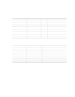
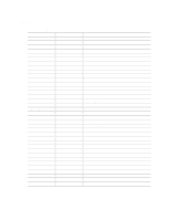
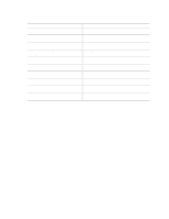
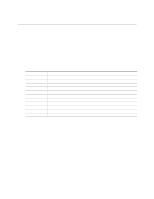
I/O Map Table 31. I/O Map Address (hex) 0000 - 000F 0020 - 0021 0040 - 0043 0060 0061 0064 0070 - 0071 0072 - 0073 0080 - 008F 0092 00A0 - 00A1 00B2 - 00B3 00C0 - 00DF 00F0 0170 - 0177 01F0 - 01F7 0228 - 022F* 0278 - 027F* 02E8 - 02EF* 02F8 - 02FF* 0376 0377, bits 6:0 0378 - 037F 03B0 - 03BB 03C0 - 03DF 03E8 - 03EF 03F0 - 03F5 03F6 03F8 - 03FF 04D0 - 04D1 LPTn + 400 0CF8 - 0CFB** 0CF9*** 0CFC - 0CFF FFA0 - FFA7 FFA8 - FFAF Size 16 bytes 2 bytes 4 bytes 1 byte 1 byte 1 byte 2 bytes 2 bytes 16 bytes 1 byte 2 bytes 2 bytes 32 bytes 1 byte 8 bytes 8 bytes 8 bytes 8 bytes 8 bytes 8 bytes 1 byte 7 bits 8 bytes 12 bytes 32 bytes 8 bytes 6 bytes 1 byte 8 bytes 2 bytes 8 bytes 4 bytes 1 byte 4 bytes 8 bytes 8 bytes Technical Reference Description DMA controller Programmable Interrupt Control (PIC) System timer Keyboard controller byte-reset IRQ System speaker Keyboard controller, CMD / STAT byte System CMOS / Real Time Clock System CMOS DMA controller Fast A20 and PIC PIC APM control DMA Numeric data processor Secondary IDE channel Primary IDE channel LPT3 LPT2 COM4 / video (8514A) COM2 Secondary IDE channel command port Secondary IDE channel status port LPT1 Video (VGA) Video (VGA) COM3 Diskette channel 1 Primary IDE channel command port COM1 Edge / level triggered PIC ECP port, LPTn base address + 400h PCI configuration address register Turbo and reset control register PCI configuration data register Primary bus master IDE registers Secondary bus master IDE registers continued 75
-
 1
1 -
2
-
3
-
4
-
5
-
6
-
7
-
8
-
9
-
10
-
11
-
12
-
13
-
14
-
15
-
16
-
17
-
18
-
19
-
20
-
21
-
22
-
23
-
24
-
25
-
26
-
27
-
28
-
29
-
30
-
31
-
32
-
33
-
34
-
35
-
36
-
37
-
38
-
39
-
40
-
41
-
42
-
43
-
44
-
45
-
46
-
47
-
48
-
49
-
50
-
51
-
52
-
53
-
54
-
55
-
56
-
57
-
58
-
59
-
60
-
61
-
62
-
63
-
64
-
65
-
66
-
67
-
68
-
69
-
 70
70 -
 71
71 -
 72
72 -
 73
73 -
 74
74 -
 75
75 -
 76
76 -
 77
77 -
 78
78 -
 79
79 -
 80
80 -
81
-
82
-
83
-
84
-
85
-
86
-
87
 |
 |