LG KM710 Service Manual - Page 15
HW Circuit Description - bands
 |
View all LG KM710 manuals
Add to My Manuals
Save this manual to your list of manuals |
Page 15 highlights
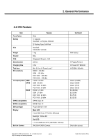
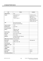
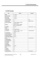
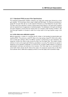
3. HW Circuit Description 3. HW Circuit Description 3.1 General Description The RF part consists of a transmitter, a receiver, a synthesizer, a voltage supply and a DCXO part. The main RF Chipset B6PLD is a highly integrated RF transceiver IC FOR Digital Interface of GSM 850,DCS1800 and PCS1900 quad-band cellular systems. The B6PLD incorporates EDGE transceiver capability, quad R low-noise amplifiers (LNAs). Direct conversion mixers, a programmable gain amplifier(PGA) with DC offset and frequency response correction, ADC, Digital filter, Digital Interface, fully integrated VCOs, an RF fractional-N synthesizer, a low-noise offset PLL transmitter, Digital modulator, TXDAC, RAMPDAC, and AFCDAC. The B6PLD includes state machine control through serial programming. All functions operate down to 2.67V and are housed in a 72- pin BGA package. Hence the B6PLD can form a small size transceiver handset for quad band EDGE transceiver. 3.2 RF Part 3.2.1 Receiver Part The B6PLD receiver supports quad band, so the front-end incorporates four LNAs and two mixers. The incoming RF signals are mixed directly down to I/Q baseband by the front-end block. This incorporates four LNAs/four buffers and two Gilbert Cell mixer blocks optimized for operation at 850MHz, 900MHz, 1800MHz and 1900MHz respectively. The front-end block is followed by two closely matched baseband amplifier chains. These include distributed low pass filtering, one switched gain stage and one fixed gain stage. In addition, the baseband section integrates A/D and D/A converters which provide automatic on-chip correction of DC offsets. LGE Internal Use Only Receiver Part Block Diagram - 16 - Copyright © 2008 LG Electronics. Inc. All right reserved. Only for training and service purposes
-
 1
1 -
2
-
3
-
4
-
5
-
6
-
7
-
8
-
9
-
 10
10 -
 11
11 -
 12
12 -
 13
13 -
 14
14 -
 15
15 -
 16
16 -
 17
17 -
 18
18 -
 19
19 -
 20
20 -
21
-
22
-
23
-
24
-
25
-
26
-
27
-
28
-
29
-
30
-
31
-
32
-
33
-
34
-
35
-
36
-
37
-
38
-
39
-
40
-
41
-
42
-
43
-
44
-
45
-
46
-
47
-
48
-
49
-
50
-
51
-
52
-
53
-
54
-
55
-
56
-
57
-
58
-
59
-
60
-
61
-
62
-
63
-
64
-
65
-
66
-
67
-
68
-
69
-
70
-
71
-
72
-
73
-
74
-
75
-
76
-
77
-
78
-
79
-
80
-
81
-
82
-
83
-
84
-
85
-
86
-
87
-
88
-
89
-
90
-
91
-
92
-
93
-
94
-
95
-
96
-
97
-
98
-
99
-
100
-
101
-
102
-
103
-
104
-
105
-
106
-
107
-
108
-
109
-
110
-
111
-
112
-
113
-
114
-
115
-
116
-
117
-
118
-
119
-
120
-
121
-
122
-
123
-
124
-
125
-
126
-
127
-
128
-
129
-
130
-
131
-
132
-
133
-
134
-
135
-
136
-
137
-
138
-
139
-
140
-
141
-
142
-
143
-
144
-
145
-
146
-
147
-
148
-
149
-
150
-
151
-
152
-
153
-
154
-
155
-
156
-
157
-
158
-
159
-
160
-
161
-
162
-
163
-
164
-
165
-
166
-
167
-
168
-
169
-
170
-
171
-
172
-
173
-
174
 |
 |
