LG KM710 Service Manual - Page 30
U-sd Controller, 4.5 Dai, 4.6 Camera & Lcd
 |
View all LG KM710 manuals
Add to My Manuals
Save this manual to your list of manuals |
Page 30 highlights
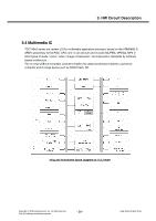
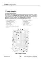
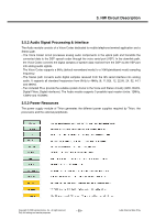
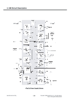
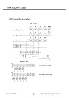
3. HW Circuit Description 3.4.4 u-SD CONTROLLER SD/MMC controller is designed to support SD specification Ver.1.01, SDIO specification Ver1.10, CEATA and MMC specification Ver.3.0. By using DMA and internal FIFO(8x32bits) data transfer rate is up to maximum speed, SD/MMC card supports. Moreover because this block has internal clock controller, it is possible to adjust operating frequency for power saving or other operating conditions just from setting special register. 3.4.5 DAI The TCC74xx provides digital audio interface that complies with IIS (Inter-IC Sound). The DAI has five input/output pins for IIS interface; MCLK, BCLK, LRCK, DAI, DAO. All DAI input/output pins are multiplexed with GPIO pins; GPIO_B. The MCLK is the system clock pin that is used for CODEC system clock. In master mode, the MCLK can be generated from clock generator in which that is known as a DCLK, or fed from the outside of chip in slave mode. The DAI can process 256fs, 384fs and 512fs as a system clock. 256fs means that the system clock has 256 times of sampling frequency (fs). The BCLK is the serial bit clock for IIS data exchange. The DAI can generate 64fs, 48fs and 32fs by dividing a system clock. The polarity of BCLK can be programmed. That is, the serial bit can be stable either rising edge of BCLK or falling edge of BCLK. The LRCK is the frame clock for the stereo audio channel Left and Right. The frequency of LRCK is known as the "fs" - sampling frequency. Generally, for audio application - such as MP3 player , CD player, the fs can be set to 8kHz, 16kHz, 11.05kHz, 24kHz, 32kHz, 44.1kHz and 48kHz. For supporting the wide range of sampling frequency in audio application, the DCO function is very useful to generate a system clock. Refer the chapter of clock generator for detail information. All three clocks (MCLK, BCLK, LRCK) are selectable as master or slave. The DAI, DAO are the serial data input output pins respectively. The DAI has two 8-word input/output buffers. It has a banked buffer structure so that one side of buffer is receiving/transmitting data while the other side of that can be read/written through the DADI_XX/DADO_XX registers. The maximum data word size is 24 bit. Data is justified to MSB of 32bits and zeros are padded to LSB. There are 2 types of interrupt from IIS; transmit done interrupt, receive done interrupt. The transmitdone interrupt is generated when the 8 words are transferred successfully in the out put buffer. At this interrupt, user should fill another 8 more words into the other part of the output buffer in the interrupt service routine (ISR). In this ISR routine, 8 consecutive stores of word data to the DADO registers are needed. The receive-done interrupt is generated when the 8 words are received successfully in the input buffer. At this interrupt, user should read 8 received words from the input buffer using 8 consecutive load instructions from the DADI registers. 3.4.6 Camera & LCD The TCC7402 provides camera interface. The features of CIF are is 8-bit data and sync line which supports CCIR 601/656, 4:2:2,YCbCr(YUV). The TCC7402 provides LCD interface. The LCD MODULE of KM710c is 2" TFT-LCD which is displayed 65000 color. The LCD controller is used to send out image data from the system memory Copyright © 2008 LG Electronics. Inc. All right reserved. Only for training and service purposes - 31 - LGE Internal Use Only
-
 1
1 -
2
-
3
-
4
-
5
-
6
-
7
-
8
-
9
-
10
-
11
-
12
-
13
-
14
-
15
-
16
-
17
-
18
-
19
-
20
-
21
-
22
-
23
-
24
-
 25
25 -
 26
26 -
 27
27 -
 28
28 -
 29
29 -
 30
30 -
 31
31 -
 32
32 -
 33
33 -
 34
34 -
 35
35 -
36
-
37
-
38
-
39
-
40
-
41
-
42
-
43
-
44
-
45
-
46
-
47
-
48
-
49
-
50
-
51
-
52
-
53
-
54
-
55
-
56
-
57
-
58
-
59
-
60
-
61
-
62
-
63
-
64
-
65
-
66
-
67
-
68
-
69
-
70
-
71
-
72
-
73
-
74
-
75
-
76
-
77
-
78
-
79
-
80
-
81
-
82
-
83
-
84
-
85
-
86
-
87
-
88
-
89
-
90
-
91
-
92
-
93
-
94
-
95
-
96
-
97
-
98
-
99
-
100
-
101
-
102
-
103
-
104
-
105
-
106
-
107
-
108
-
109
-
110
-
111
-
112
-
113
-
114
-
115
-
116
-
117
-
118
-
119
-
120
-
121
-
122
-
123
-
124
-
125
-
126
-
127
-
128
-
129
-
130
-
131
-
132
-
133
-
134
-
135
-
136
-
137
-
138
-
139
-
140
-
141
-
142
-
143
-
144
-
145
-
146
-
147
-
148
-
149
-
150
-
151
-
152
-
153
-
154
-
155
-
156
-
157
-
158
-
159
-
160
-
161
-
162
-
163
-
164
-
165
-
166
-
167
-
168
-
169
-
170
-
171
-
172
-
173
-
174
 |
 |
