LG KM710 Service Manual - Page 38
Pin Description
 |
View all LG KM710 manuals
Add to My Manuals
Save this manual to your list of manuals |
Page 38 highlights
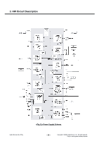
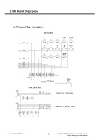
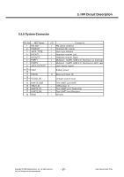
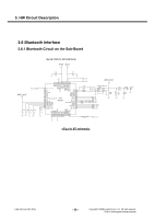
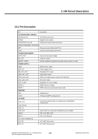
3. HW Circuit Description 3.6.2 Pin Description Pin Description CLOCKS/GLOBAL SIGNALS SLOW-CLK_IN 32.768.kHz clock input XTALM Negative fast crystal in XTALP/FAST_CLK_IN Positive fast crystal in/fast clock input RADIO FREQUENCY INTERFACE RFP Receiver/transmit differential RF I/O RFM Receiver/transmit differential RF/IO POWER MANAGEMENT VLDC_OUT Very-low drop-output voltage KA_OUT Keep alive output NSHUT_DOWN Devices shutdown input(active low) also acts as power-on reset POWER SUPPLY VBAT Battery power supply VDD_IO1 Power supply for I/O BB_LDO_OUT1 Baseband LDO output ANA_LDO_OUT Analog LDO output RFIO_LDO_OUT RFIO LDO output, power source for RF elements OSC_LDO_OUT OSC LDO output VDD_IN_BB Baseband LDO input voltage BGAP_V BGAP reference voltage BGAP_I BGAP reference current(used only for test) GROUND VSS Digital ground VSSA Analog ground/RF analog ground I/O NAME AUD_CLK Input-when external codec is configured as master(default configuration) AUD_FSYNC AUD_IN AUD_OUT High Z with PD, except when transmitting voice samples GPIO0 EXT_CLK_REQ_OUT GPIO1 EXT_CLK_REQ_IN HCI UART INTERFACE HCI_RX HCI UART data receive HCI_TX HCI UART data transmit Copyright © 2008 LG Electronics. Inc. All right reserved. Only for training and service purposes - 39 - LGE Internal Use Only
-
 1
1 -
2
-
3
-
4
-
5
-
6
-
7
-
8
-
9
-
10
-
11
-
12
-
13
-
14
-
15
-
16
-
17
-
18
-
19
-
20
-
21
-
22
-
23
-
24
-
25
-
26
-
27
-
28
-
29
-
30
-
31
-
32
-
 33
33 -
 34
34 -
 35
35 -
 36
36 -
 37
37 -
 38
38 -
 39
39 -
 40
40 -
 41
41 -
 42
42 -
 43
43 -
44
-
45
-
46
-
47
-
48
-
49
-
50
-
51
-
52
-
53
-
54
-
55
-
56
-
57
-
58
-
59
-
60
-
61
-
62
-
63
-
64
-
65
-
66
-
67
-
68
-
69
-
70
-
71
-
72
-
73
-
74
-
75
-
76
-
77
-
78
-
79
-
80
-
81
-
82
-
83
-
84
-
85
-
86
-
87
-
88
-
89
-
90
-
91
-
92
-
93
-
94
-
95
-
96
-
97
-
98
-
99
-
100
-
101
-
102
-
103
-
104
-
105
-
106
-
107
-
108
-
109
-
110
-
111
-
112
-
113
-
114
-
115
-
116
-
117
-
118
-
119
-
120
-
121
-
122
-
123
-
124
-
125
-
126
-
127
-
128
-
129
-
130
-
131
-
132
-
133
-
134
-
135
-
136
-
137
-
138
-
139
-
140
-
141
-
142
-
143
-
144
-
145
-
146
-
147
-
148
-
149
-
150
-
151
-
152
-
153
-
154
-
155
-
156
-
157
-
158
-
159
-
160
-
161
-
162
-
163
-
164
-
165
-
166
-
167
-
168
-
169
-
170
-
171
-
172
-
173
-
174
 |
 |
