Lexmark 3350 Service Manual - Page 63
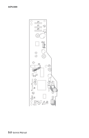
Locations and connections, System board
 |
View all Lexmark 3350 manuals
Add to My Manuals
Save this manual to your list of manuals |
Page 63 highlights
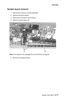
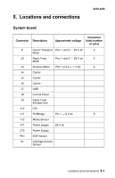
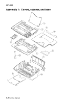
5. Locations and connections 4479-XXX System board Connector Description Approximate voltage Connector (total number of pins) J1 Carrier Transport Pins 1 and 2 - 29 V dc 2 Motor J2 Paper Feed Pins 1 and 2 - 29 V dc 2 Motor J3 Scanner Motor Pins 1,2,3,4 - 1 V dc 4 J4 Carrier J5 Carrier J6 Carrier J7 USB J8 Control Panel J9 Paper Feed Encoder Dial J10 CIS J11 PictBridge Pin 1 - 9 V dc 5 J12 Media Sensor JT1 Power Supply 29 V dc JT2 Power Supply PS1 EOF Sensor S1 Cartridge Access Sensor Locations and connections 5-1
-
 1
1 -
2
-
3
-
4
-
5
-
6
-
7
-
8
-
9
-
10
-
11
-
12
-
13
-
14
-
15
-
16
-
17
-
18
-
19
-
20
-
21
-
22
-
23
-
24
-
25
-
26
-
27
-
28
-
29
-
30
-
31
-
32
-
33
-
34
-
35
-
36
-
37
-
38
-
39
-
40
-
41
-
42
-
43
-
44
-
45
-
46
-
47
-
48
-
49
-
50
-
51
-
52
-
53
-
54
-
55
-
56
-
57
-
 58
58 -
 59
59 -
 60
60 -
 61
61 -
 62
62 -
 63
63 -
 64
64 -
 65
65 -
 66
66 -
 67
67 -
 68
68 -
69
-
70
-
71
-
72
-
73
-
74
-
75
-
76
 |
 |

4479-XXX
Locations and connections
5-1
5.
Locations and connections
System board
Connector
Description
Approximate voltage
Connector
(total number
of pins)
J1
Carrier Transport
Motor
Pins 1 and 2 – 29 V dc
2
J2
Paper Feed
Motor
Pins 1 and 2 – 29 V dc
2
J3
Scanner Motor
Pins 1,2,3,4 – 1 V dc
4
J4
Carrier
J5
Carrier
J6
Carrier
J7
USB
J8
Control Panel
J9
Paper Feed
Encoder Dial
J10
CIS
J11
PictBridge
Pin 1 – 9 V dc
5
J12
Media Sensor
JT1
Power Supply
29 V dc
JT2
Power Supply
PS1
EOF Sensor
S1
Cartridge Access
Sensor