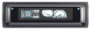
Sony CDX-M800 Service Manual - Page 19
Pin No., Pin Name, Pin Description - no power
 |
View all Sony CDX-M800 manuals
Add to My Manuals
Save this manual to your list of manuals |
Page 19 highlights
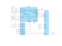
Pin No. 51 52 53 54 55 56 57 58 59 60 61 62 63 64 65 66 67 68 69 70 71 72 73 74 75 76 77 78 79 80 81 82 83 84 85 86 87 88 89 90 91 92 93 94 95 96 97 98 99 100 Pin Name DST SEL2 CD LM LO CD LM EJ CD RST CD AO CD STB CD TSTB CD RFOK CD XTALEN VCC2 RESET OUT VSS TEST IN BUS ON SYS RST BUS/AUX LINK OFF ACC IN ILL IN RC IN1 NCO CD SELF SW TU ATT IN CLOSE SW OPEN SW I-DET MOT- MOT+ ROMC EN QUALITY MPTH VSM SA IN KEY IN1 KEY IN0 RC IN0 KEY ACK2 KEY ACK0 KEY ACK1 OPEN KEY RAM BU FLD ON FL ON AVSS DISP CE VREF AVCC DISP SI/RX DISP SO/TX DISP CKO I/O Pin Description I Destination select signal input O CD loading motor control signal output O CD eject motor control signal output O CD servo reset signal output O CD servo command/parameter discri. output O CD servo data strobe signal output O CD servo text strobe signal output I CD servo RFOK signal input O CD servo crystal OSC control signal output - Power supply pin (+5V) O Display CPU reset signal output - Ground I Test mode setting detect signal input O BUS ON control signal output O System reset signal output O BUS/AUX select control signal output O Link OFF control signal output I Accessory key ON detect signal input I Ilumination line detect signal input I Rotary commander signal input 1 O Not used. (Open) I CD self SW detect signal input I Tuner mute control signal input I Front panel close detect signal input I Front panel open detect signal input I Front panel current detect signal input O Front panel open/close control signal output O Front panel open/close control signal output I ROM correction enable signal input I Tuner noise detect signal input I Tuner multi-path signal input I S-meter signal input I SA data input I Key signal input 1 I Key signal input 0 I Rotary commander signal input 0 I Key acknowledge detect signal input 2 I Key acknowledge detect signal input 0 I Key acknowledge detect signal input 1 I Open key detect signal input I RAM reset detect signal input O FL driver power supply ON/OFF signal output O FL power supply ON/OFF signal - Ground O Display CPU chip enable output - A/D converter reference voltage (+5V) - Power supply pin (+5V) I Display CPU BUS data input O Display CPU BUS data output O Display CPU BUS clock output CDX-M800 19
-
 1
1 -
2
-
3
-
4
-
5
-
6
-
7
-
8
-
9
-
10
-
11
-
12
-
13
-
 14
14 -
 15
15 -
 16
16 -
 17
17 -
 18
18 -
 19
19 -
 20
20 -
 21
21 -
 22
22 -
 23
23 -
 24
24 -
25
-
26
-
27
-
28
-
29
-
30
-
31
-
32
-
33
-
34
-
35
-
36
-
37
-
38
-
39
-
40
-
41
-
42
-
43
-
44
-
45
-
46
-
47
-
48
-
49
-
50
-
51
-
52
-
53
-
54
 |
 |
