Sony CDX-M800 Service Manual - Page 24
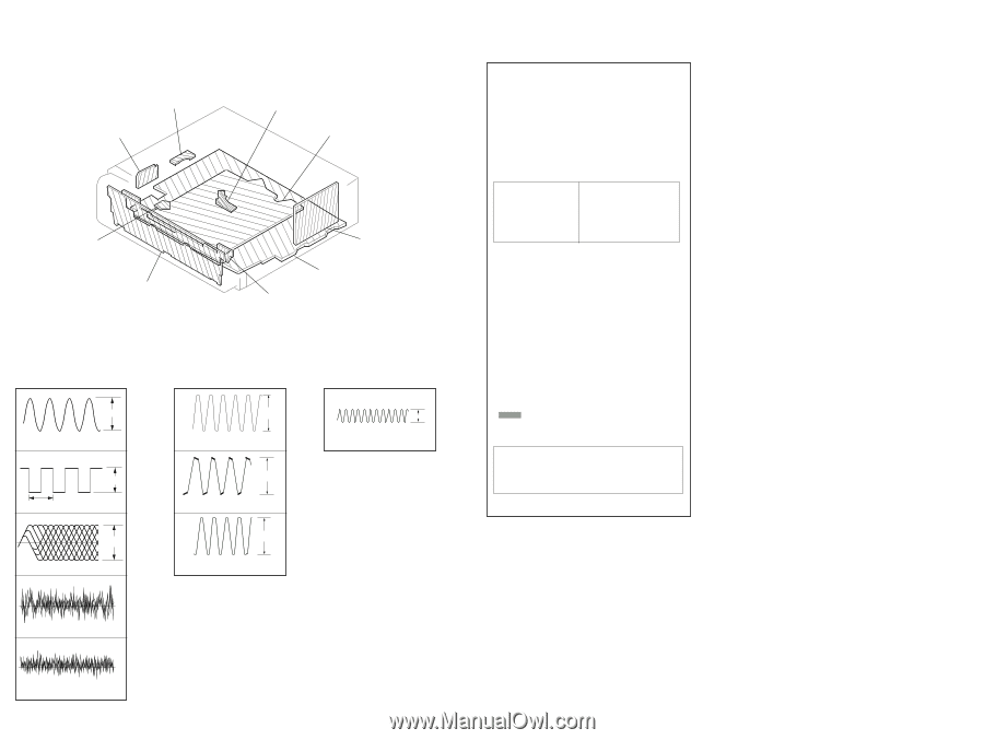
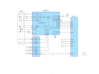
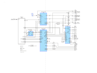
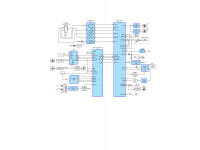
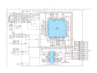
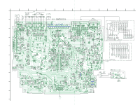
CIRCUIT BOARDS LOCATION, Waveforms, tuner unit, TUX501, IN SELF SW board, SWITCH board, LOAD SW board
 |
View all Sony CDX-M800 manuals
Add to My Manuals
Save this manual to your list of manuals |
Page 24 highlights
CDX-M800 4-5. CIRCUIT BOARDS LOCATION IN SELF SW board SWITCH board SL SW board SERVO board LOAD SW board DISPLAY board SUB board tuner unit (TUX501) MAIN board • Waveforms - Servo Board - (MODE: CD PLAY) 1 2Vp-p 16.9344MHz IC1 wd (XTAL) 2 5Vp-p 3.2msec IC1 ts (PACK) 3 1.2Vp-p IC1 uj (RFO) 4 0V Approx. 100mVp-p IC1 oa (FEO) 5 0V Approx. 100mVp-p IC1 od (TEO) • Waveforms - Main Board - (MODE: FM) 1 3.2Vp-p 4.3MHz IC502 4 (OSCD) 2 1.8Vp-p 32.768kHz IC303 9 (XOUT) 3 3.6Vp-p 6MHz IC303 qa (OSCOUT) • Waveform - Display Board - (MODE: FM) 1 1.5Vp-p 30MHz IC2 qa (XOUT) 24 THIS NOTE IS COMMON FOR PRINTED WIRING BOARDS AND SCHEMATIC DIAGRAMS. (In addition to this, the necessary note is printed in each block.) for schematic diagram: • All capacitors are in µF unless otherwise noted. pF: µµF 50 WV or less are not indicated except for electrolytics and tantalums. • All resistors are in Ω and 1/4 W or less unless otherwise specified. • % : indicates tolerance. • f : internal component. • C : panel designation. Note: The components identified by mark 0 or dotted line with mark 0 are critical for safety. Replace only with part number specified. Note: Les composants identifiés par une marque 0 sont critiques pour la sécurité. Ne les remplacer que par une piéce portant le numéro spécifié. • A : B+ Line. • Power voltage is dc 14.4V and fed with regulated dc power supply from ACC and BATT cords. • Voltages are taken with a VOM (Input impedance 10 MΩ). Voltage variations may be noted due to normal production tolerances. • Waveforms are taken with a oscilloscope. Voltage variations may be noted due to normal production tolerances. • Circled numbers refer to waveforms. • Signal path. F : FM f : AM/MW/LW J : CD • Abbreviation CND : Canadian model for printed wiring boards: • X : parts extracted from the component side. • Y : parts extracted from the conductor side. • x : parts mounted on the conductor side. • a : Through hole. • : Pattern from the side which enables seeing. (The other layer's patterns are not indicated.) Caution: Pattern face side: Parts on the pattern face side seen from the (Side B) pattern face are indicated. Parts face side: Parts on the parts face side seen from the (Side A) parts face are indicated. • Abbreviation CND : Canadian model 24
-
 1
1 -
2
-
3
-
4
-
5
-
6
-
7
-
8
-
9
-
10
-
11
-
12
-
13
-
14
-
15
-
16
-
17
-
18
-
 19
19 -
 20
20 -
 21
21 -
 22
22 -
 23
23 -
 24
24 -
 25
25 -
 26
26 -
 27
27 -
 28
28 -
 29
29 -
30
-
31
-
32
-
33
-
34
-
35
-
36
-
37
-
38
-
39
-
40
-
41
-
42
-
43
-
44
-
45
-
46
-
47
-
48
-
49
-
50
-
51
-
52
-
53
-
54
 |
 |