Sony MDSJE320 Service Manual
Sony MDSJE320 - MiniDisc Recorder Manual
 |
UPC - 027242541344
View all Sony MDSJE320 manuals
Add to My Manuals
Save this manual to your list of manuals |
Sony MDSJE320 manual content summary:
- Sony MDSJE320 | Service Manual - Page 1
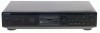
SERVICE MANUAL MDS-JE320 US Model Canadian Model AEP Model Model Name Using Similar Mechanism MDS-JE510 MD Mechanism Type MDM-3GC Optical Pick-up Type KMS-260A/J1NP SPECIFICATIONS MICROFILM MINIDISC DECK - Sony MDSJE320 | Service Manual - Page 2
batteries according to manufacture's instructions. ADVARSEL! Lithiumbatteri - . Flexible Circuit Board Repairing • Keep the temperature of soldering iron around 270˚C during repairing. • Do not SONY PARTS WHOSE PART NUMBERS APPEAR AS SHOWN IN THIS MANUAL OR IN SUPPLEMENTS PUBLISHED BY SONY. - Sony MDSJE320 | Service Manual - Page 3
the original service problem, perform Simpson 229 or RCA WT-540A. Follow the manufacturers' instructions to use these instruments. 2. A battery-operated AC 63 7-2. Front Panel Section 64 7-3. Mechanism Deck Section (1) (MDM-3GC 65 7-4. Mechanism Deck Section (2) (MDM-3GC 66 8. ELECTRICAL PARTS - Sony MDSJE320 | Service Manual - Page 4
error codes which show the error history in the test mode during servicing.For detail on how to view error codes for users, refer to the following box in the instruction manual. Self-Diagnosis Function The deck has a self-diagnosis display. This function shows a three-digit display (a combination of - Sony MDSJE320 | Service Manual - Page 5
SECTION 1 SERVICING NOTE JIG FOR CHECKING BD BOARD WAVEFORM The special jig (J-2501- for checking the signal RF : RF signal (Check jitter) RF VC TEO IOP I + 3V CN110 Mechanism deck Jig (J-2501-124-A) FORCED RESET The system microprocessor can be reset in the following way. Use these methods when - Sony MDSJE320 | Service Manual - Page 6
number. • The display of the DRAM data amount enables data reading, accumulation, ejection, and writing to be performed smoothly. If writing is not smooth, data may decrease considerably. Method: 1. Load a recordable disc whose contents can be erased into the unit. 2. Press the EDIT/NO button - Sony MDSJE320 | Service Manual - Page 7
Reading the Retry Cause Display Higher Bits Lower Bits Hexa- Hexadecimal 8 4 2 1 8 4 2 1 Bit decimal b7 b6 b5 b4 b3 b2 b1 b0 Cause of Retry Binary 0 0 0 0 0 0 0 0 00 Spindle is slow 0 0 0 0 0 0 0 1 01 (Not used) 0 0 0 0 0 0 1 0 02 ader5 Occurring conditions When spindle rotation is - Sony MDSJE320 | Service Manual - Page 8
) switch 2 Remote sensor 3 Display window 4 Disc compartment 5 AMS knob 6 0/) buttons 7 DISPLAY/CHAR button 8 INPUT switch !∞ !¢ !£ 9 REC LEVEL knob !£ r REC (recording) button !¢ p (stop) button !∞ P (pause) button !§ · (play) button !¶ YES button !• EDIT/NO button !ª § EJECT button - 8 - - Sony MDSJE320 | Service Manual - Page 9
SECTION 3 DISASSEMBLY Note : Follow the disassembly procedure in the numerical order given. 3-1. CASE AND FRONT PANEL ASSEMBLY 1 Two screws (Case 3 TP 2) 4 Case 3 Screw (case 3 TP 2) 5 Ground terminal claw 2 Two screws (Case 3 TP 2) 9 Remove the front panel assembly releasing two claws. 8 Four - Sony MDSJE320 | Service Manual - Page 10
3-3. BD BOARD 2 Flat type wire (15 core) 4 OP relay flexible board 5 BD board 1 Flexible board (Over write head) 3 Screw (BVTT2×4) 3-4. SUB CHASSIS 1 Two step screws 3 Two insulators 2 Two step screws 4 Two insulators Part A NG Part A 5 Sub chassis Part A OK Take care so that the part A - Sony MDSJE320 | Service Manual - Page 11
3-5. SHUTTER ASSEMBLY 1 Stepper washer 2 Shaft (shutter) 3 Shutter assembly Shutter assembly Shaft (lid) Shaft (shutter) Hole B Hole A When installing, install the shaft (shutter) into the hole A as shown in the figure before installing the shaft (lid) into the hole B. 3-6. OVER WRITE HEAD 1 - Sony MDSJE320 | Service Manual - Page 12
3-7. SLIDER COMPLETE ASSEMBLY claw claw 4 Remove the slider complete assembly in the direction of arrow with putting out of two claws. 1 Screw (M1.7×2) 3 Set the shaft of Gear (LA) to be at the position in the figure. 45° 2 Retainer (gear) • Note for Installation of Slider Complete Assembly - Sony MDSJE320 | Service Manual - Page 13
EJECT button is pressed while the disc is rotating during continuous playback, continuous recording, etc., the disc will not stop rotating. Therefore, it will be ejected while rotating. Be sure to press the §EJECT curve CHECK, MANUAL CMD and SVDATA READ are not used in servicing. If set accidentally - Sony MDSJE320 | Service Manual - Page 14
and REC goes off. 2 Press the §EJECT button to remove the disc. Note 1 : The recording start addresses for IN, MID, and OUT recording, be careful not to apply vibration. 4-5-3. Non-Volatile Memory Mode This mode reads and writes the contents of the non-volatile memory. It is not used in servicing - Sony MDSJE320 | Service Manual - Page 15
gain display and the IVR display are not used for servicing. 1. MODE display Displays "TEMP ADJUST", "CPLAY MODE error AD = : Indicates ADER 3. Address display Addresses are displayed as follows. (MO : Recordable disc, CD : Disc for playback only) h= s = (MO pit and CD) h= a = (MO groove) - Sony MDSJE320 | Service Manual - Page 16
do not connect inside the MD laser power meter 8010S (J-2501-145-A) instead of the conventional laser power meter is convenient. It sharply reduces the time and trouble to set the laser power meter sensor onto the objective lens of the pick-up. 5-4. CREATING CONTINUOUSLY RECORDED DISC • This disc - Sony MDSJE320 | Service Manual - Page 17
the objective lens of the optical pick-up. (When it cannot be set properly, press the 0 button or ) button to move the optical pick-up.) Connect the digital volt meter to CN110 pin 5 (I+3V) and CN110 pin 4 (IOP). 2. Rotate the AMS knob and display "LDPWR ADJUST". (Laser power : For adjustment - Sony MDSJE320 | Service Manual - Page 18
"EFBAL ADJUST" will be displayed. 18. Press the §EJECT button and remove the check disc (MD) TDYS-1. Note 1 : MO reading data will be erased during if a recorded disc is used in this adjustment. Note 2 : If the traverse waveform is not clear, connect the oscilloscope as shown in the following figure - Sony MDSJE320 | Service Manual - Page 19
is not above 00 every time. 9. Press the EDIT/NO button, next press the §EJECT button, and remove the continuously recorded disc. Note 1 : If the C1 error and ADER are above 00 at points a ( use the jig. for checking the waveform. (Refer to Servicing Note on page 4.) MDS-JE320 - 19 - - 20 - - Sony MDSJE320 | Service Manual - Page 20
MDS-JE320 6-1. BLOCK DIAGRAMS - BD Section - • Signal path : PB : REC : PB (Digital out) : REC (Digital in) SECTION 6 DIAGRAMS HR901 OVER WRITE HEAD 11 HEAD 14 DRIVE Q181,182 15 17 OVER WRITE HEAD DRIVE IC181 3 18 9 1 18 Q180 2 OPTICAL PICK-UP BLOCK (KMS-260A/J1NP) DETECTOR F I CB - Sony MDSJE320 | Service Manual - Page 21
MDS-JE320 - MAIN Section - DIN IC314 12 13 DIGITAL OPTICAL IN 3 IC353 ADDT DADT SCTX XINT BCK LRCK 512FS SQSY DQSY MNT3 MNT2 MNT1 MNT0 SENS SRDT SCLK SWDT XLAT BD SECTION LIMIT REFLECT PROTECT CHUCK IN PACK-OUT PB-P REC-P BCK LRCK 512FS SCLK SWDT XLAT LDON WRPWR MOD LOAD-IN 2 DRIVE 12 - Sony MDSJE320 | Service Manual - Page 22
MDS-JE320 6-2. CIRCUIT BOARDS LOCATION SW board DISPLAY board BD board EJECT SW board CONTROL (SW) IC307 0 (LRCK1), @• (LRCK2) • U : B+ Line. • V : B- Line. • H : adjustment for repair. • Voltages and waveforms are dc with respect to ground under no-signal (detuned) conditions. No mark : FM ( ) - Sony MDSJE320 | Service Manual - Page 23
IC152 B-12 IC171 F-9 IC181 D-9 IC192 G-6 Q101 C-14 Q102 B-15 Q103 B-14 Q104 B-14 Q162 B-14 Q163 B-15 Q180 D-6 Q181 B-9 Q182 B-9 (Page 45) 16 (Page 33) MDS-JE320 (Page 33) - 27 - - 28 - - Sony MDSJE320 | Service Manual - Page 24
MDS-JE320 6-4. Schematic Diagram - BD Section (1/2)- • See page 26 for Waveforms. • See page 49 for IC Block Diagrams. • See page 54 for IC Pin Functions. 16 (Page 31) - 29 - (Page 32) - 30 - - Sony MDSJE320 | Service Manual - Page 25
6-5. Schematic Diagram - BD Section (2/2) - • See page 26 for Waveforms. • See page 49 for IC Block Diagrams. • See page 54 for IC Pin Functions. (Page 29) (Page 30) MDS-JE320 BR24C01AF 16 (Page 36) (Page 47) (Page 35) - 31 - - 32 - - Sony MDSJE320 | Service Manual - Page 26
MDS-JE320 6-6. Printed Wiring Board - Main Section - • See page 25 for Circuit Boards Location. • Semiconductor Location Ref. No. Location 1 2 3 D301 G-11 D302 G-11 D303 G-10 D304 G-10 A - Sony MDSJE320 | Service Manual - Page 27
6-7. Schematic Diagram - Main Section (1/3) - • See page 26 for Waveforms • See page 54 for IC Pin Functions. MDS-JE320 (PAGE 32) - 35 - (PAGE 31) - 36 - - Sony MDSJE320 | Service Manual - Page 28
MDS-JE320 6-8. Schematic Diagram - Main Section (2/3) - • See page 26 for Waveforms. • See page 49 for IC Block Diagrams. • See page 54 for IC Pin Functions. - 37 - - 38 - - Sony MDSJE320 | Service Manual - Page 29
6-9. Schematic Diagram - Main Section (3/3) - • See page 49 for IC Block Diagram. MDS-JE320 (PAGE 44) - 39 - - 40 - - Sony MDSJE320 | Service Manual - Page 30
MDS-JE320 6-10. Printed Wiring Board - DISPLAY Section - • See page 25 for Circuit Boards Location. 1 2 3 4 ANALOG C (PAGE 33) S762 DISPLAY/CHAR S774 S775 AMS (PUSH ENTER) 5 4 1 3 EJECT SW BOARD 1 S776 EJECT 3 CN705 21 1-661-893- (21) 1 3 I S771 S772 S780 S781 S752 S751 REC - Sony MDSJE320 | Service Manual - Page 31
6-11. Schematic Diagram - DISPLAY Section - • See page 26 for Waveforms. - 43 - MDS-JE320 (PAGE 39) - 44 - - Sony MDSJE320 | Service Manual - Page 32
MDS-JE320 6-12. Printed Wiring Board - Switch Section - • See page 25 for Circuit Boards Location. 1 2 3 4 5 6 7 8 9 10 11 12 13 A B C (Page 28) D E F G H I J 16 - 45 - - 46 - - Sony MDSJE320 | Service Manual - Page 33
6-13. Schematic Diagram - Switch Section - (Page 31) 16 - 47 - MDS-JE320 - 48 - - Sony MDSJE320 | Service Manual - Page 34
6-14. IC BLOCK DIAGRAMS • BD section IC101 CXA2523R + MORFO - MORFI RFO OPN OPO ADDC COMPP COMPO AGCI RF AGC RF PEAK I1 J2 CVB VC 3 A4 IVR - + 48 RFA1 + - 47 46 45 44 USROP - + RFA2 - -- - 1 2 HLPT -1 -2 43 42 41 40 39 38 37 + RF AGC EQ - USRC DET EQ BPF3T 3T PEAK3T P-P CFST - Sony MDSJE320 | Service Manual - Page 35
IC121 CXD2652AR SFDR SRDR FS4 FRDR FFDR DVDD TFDR TRDR LDDR APCREF DTRF CKRF XLRF F0CNT ADFG APC DCHG EFMO DVSS TEST3 TEST2 TEST1 FGIN SPFD SPRD 100 99 98 97 96 95 94 93 92 91 90 89 88 87 86 85 84 83 82 81 80 79 78 77 76 AUTO SEQUENCER MNT0 1 MNT1 2 MNT2 3 MNT3 4 SWDT 5 SCLK 6 XLAT 7 SRDT 8 - Sony MDSJE320 | Service Manual - Page 36
IC171 XL24C01AF A0 1 A1 2 1024 BIT EEPROM ARRAY 7BIT ADDRESS DECODER 7BIT SLAVE WORD ADDRESS RESISTOR 8BIT DATA RESISTOR 8 VCC 7 TEST A2 3 START STOP CONTROL CIRCUIT 6 SCL ACK GND 4 HIGH VOLTAGE VOLTAGE GENERATION CIRCUIT DET 5 SDA IC192 L88MS33T START UP CIRCUIT REFERENCE - Sony MDSJE320 | Service Manual - Page 37
IC308 M5218AL 1 2 3 4 5 6 7 8 V- V+ IC309 LA5620 IC310 M5293L GND 2 ON/OFF 4 REFERENCE VOLTAGE IN 1 + - OVERHEAT PROTECTION 5k 5 REFERENCE VOLTAGE 27k 3 OUT OVERCURRENT LIMITTER -+ 3.3V -+ -+ -+ -+ DELAY CIRCUIT VREF -+ DELAY CIRCUIT 1 2 3 4 5 6 7 PH5 STBY VCC - Sony MDSJE320 | Service Manual - Page 38
BPF22 Tracking error signal output to the CXD2650R or CXD2652AR External capacitor connection pin for the sled error signal LPF Sled error signal output cutting the low band of the ADIP amplifier User operation amplifier output (Not used) User operation amplifier inversion input (Fixed at "L") RF - Sony MDSJE320 | Service Manual - Page 39
msec Almost all, "H" is output 13 RECP 14 XINT I Laser power switching input from the system control "H": Recording, "L": Playback O Interrupt status output to the system control 15 TX I Recording data output enable input from the system control 16 OSCI I System clock input (512Fs=22.5792 MHz - Sony MDSJE320 | Service Manual - Page 40
recording/playback EFM master PLL I (A) Filter input for the recording/playback EFM master PLL O (A) Filter output for the recording Auxiliary A/D input (Fixed at "L") I (A) Connected to +3V power supply I (A) Error signal (Not used) O Tracking servo drive PWM output (-) • Abbreviation EFM: - Sony MDSJE320 | Service Manual - Page 41
(X'tal) (Not used) O Sled servo drive PWM output (-) O Sled servo drive PWM output (+) O Spindle servo drive PWM output (-) O Spindle servo drive PWM output (+) I (S) I Test input (Fixed at "L") - Ground (Digital) O EFM output when recording • Abbreviation EFM: Eight to Fourteen Modulation - Sony MDSJE320 | Service Manual - Page 42
• IC307 A/D, D/A converter (CXD8607N) Pin No. Pin Name I/O 1 INRP I 2 INRM I 3 REFI I 4 AVDD - 5 AVss - 6 APD I 7 NU - 8 NU - 9 TEST1 I 10 LRCK1 I 11 BCK1 I 12 ADDT O 13 V35A - 14 VSS1 (LF) - 15 MCKI I 16 DPD I 17 VSS2 (LF) - 18 INIT I 19 MODE I - Sony MDSJE320 | Service Manual - Page 43
Pin No. 41 42 43 44 45 46 47 48 49 50 51 52 53 54 55 56 Pin Name L1 VDD2 VDD1 VDD1 VSS1 TEST2 TEST3 VSS1 (LF) NU NU AVSS (LF) LVDD LVSS REFO INLM INLP I/O Function O Lch PLM output 1 - +5V power supply (D/A, digital) - - +5V power supply (A/D, digital) - Ground (A/D, digital) I I Test pin ( - Sony MDSJE320 | Service Manual - Page 44
Chucking 7 PACK IN I Detection input from the disc detection switch 8 PACK OUT I Detection input from the DOWN signal input "L": Down 14 REMOCON I Remote control signal interrupt input 15 SQSY ATP address I Detection signal input from the recording position detection switch 38 PLAY P - Sony MDSJE320 | Service Manual - Page 45
Monitor 3 input from the CXD2650R or CXD2652AR O Drive output to the POWER ON/STANDBY display LED - used - - I Not used O Audio bus/remote control switching signal output (Not used) - - groove detection input "H" is input for the playback only disc or TOC area (Not used) FOK signal input from - Sony MDSJE320 | Service Manual - Page 46
used - Not used O Line out muting output O O Loading motor control output *1 Detection input from the limit switch I Sled limit-In: "L" Recording-protection claw detection input from the protection detection switch I Protect: "H" Disk reflection rate detection input from the reflect detection switch - Sony MDSJE320 | Service Manual - Page 47
not stocked since they are seldom required for routine service. Some delay should be anticipated when ordering these 6 TR301 7 #2 #1 Ref. No. *1 2 3 4 *5 #1 Part No. Description 3-703-353-05 SUPPORT, PC BOARD 4-210-291-01 SCREW (CASE 3 TP2) 4-983-661-01 CASE (408226) 3-703-571-11 BUSHING - Sony MDSJE320 | Service Manual - Page 48
4-983-657-01 KNOB (AMS) 4-983-651-01 WINDOW (DISPLAY) Remark 4-963-404-21 EMBLEM (5-A), SONY A-4724-246-A DISPLAY BOARD, COMPLETE (US,CND) A-4724-275-A DISPLAY BOARD, COMPLETE (AEP) 4-951- BUTTON (MAIN) 1-661-893-11 EJECT SW BOARD Remark 63 4-977-593-11 RING (DIA. 50), ORNAMENTAL (AEP) - 64 - - Sony MDSJE320 | Service Manual - Page 49
7-3. MECHANISM DECK SECTION (1) (MDM-3GC) not supplied #3 #3 not supplied #3 201 201 202 202 not supplied #3 203 204 205 206 Ref. No. 201 202 203 204 205 Part - Sony MDSJE320 | Service Manual - Page 50
7-4. MECHANISM DECK SECTION (2) (MDM-3GC) 252 #3 #3 #5 #7 not supplied 253 not supplied 254 259 257 260 256 258 251 261 255 #6 #5 271 #6 not supplied 262 M901 263 M902 - Sony MDSJE320 | Service Manual - Page 51
parts, so they may have some difference from the original one. • Items marked "*" are not stocked since they are seldom required for routine service. Some delay should be anticipated when ordering these items. • RESISTORS All resistors are in ohms METAL: Metal-film resistor METAL OXIDE: Metal Oxide - Sony MDSJE320 | Service Manual - Page 52
BD Ref. No. IC124 IC152 IC171 IC181 IC192 Part No. Description 8-759-473-29 IC MN41V4400SJ-08-T1 8-759-430-25 IC BH6511FS-E2 8-759-484-73 IC BR24C01AF-E2 8-759-095-65 IC TC74ACT540FS 8-759-426-95 IC L88MS33T-TL Remarks Ref. No. R137 R140 R141 R142 R143 Part No. Description 1-216-025-91 RES, - Sony MDSJE320 | Service Manual - Page 53
CONTROL (SW) DISPLAY Ref. No. * Part No. Description Remarks A-4724-247-A CONTROL(SW) BOARD, COMPLETE (US,CND Ref. No. * Part No. Description Remarks A-4724-246-A DISPLAY BOARD, COMPLETE (US,CND * A-4724-276-A CONTROL(SW) BOARD, COMPLETE (AEP) * A-4724-275-A DISPLAY BOARD, COMPLETE - Sony MDSJE320 | Service Manual - Page 54
SW BOARD Remarks < CONNECTOR > CN705 1-766-806-11 HOUSING, CONNECTOR 3P < SWITCH > S776 1-554-303-21 SWITCH, TACTILE (EJECT Ref. No. C313 C314 C315 C316 C317 C318 C319 C322 C323 C324 Part No. Description 1-164-159-11 1-126-926-11 1-164-159-11 1-126- - Sony MDSJE320 | Service Manual - Page 55
Ref. No. D306 D307 D308 D309 D310 Part No. Description 8-719-024-99 8-719-024-99 8-719-109-89 8-719-024-99 8-719-024-99 DIODE DIODE DIODE DIODE DIODE 11ES2-NTA2B 11ES2-NTA2B RD5.6ESB2 11ES2-NTA2B 11ES2-NTA2B Remarks Ref. No. R115 R116 R117 R118 R119 Part No. Description 1-249-429-11 1-249- - Sony MDSJE320 | Service Manual - Page 56
MDS-JE320 WIRE (FLAT TYPE) (15 CORE) 8-583-028-02 OPTICAL PIC-UP KMS-260A/J1NP 1-500-396-11 HEAD, OVER WRITE , CONNECTION MANUAL, INSTRUCTION (ENGLISH/FRENCH) MANUAL, INSTRUCTION (AEP) (CHINESE/DUTCH/ITALIAN) MANUAL, INSTRUCTION ( 9-922-894-11 Sony Corporation Home A&V Products Company - 72 -
-
 1
1 -
 2
2 -
 3
3 -
 4
4 -
 5
5 -
 6
6 -
 7
7 -
8
-
9
-
10
-
11
-
12
-
13
-
14
-
15
-
16
-
17
-
18
-
19
-
20
-
21
-
22
-
23
-
24
-
25
-
26
-
27
-
28
-
29
-
30
-
31
-
32
-
33
-
34
-
35
-
36
-
37
-
38
-
39
-
40
-
41
-
42
-
43
-
44
-
45
-
46
-
47
-
48
-
49
-
50
-
51
-
52
-
53
-
54
-
55
-
56
 |
 |

MDS-JE320
US Model
Canadian Model
AEP Model
SERVICE MANUAL
MICROFILM
Model Name Using Similar Mechanism
MDS-JE510
MD Mechanism Type
MDM-3GC
Optical Pick-up Type
KMS-260A/J1NP
MINIDISC DECK
SPECIFICATIONS