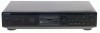
Sony MDSJE320 Service Manual - Page 44
Sony MDSJE320 - MiniDisc Recorder Manual
 |
UPC - 027242541344
View all Sony MDSJE320 manuals
Add to My Manuals
Save this manual to your list of manuals |
Page 44 highlights
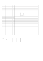
• IC316 System Control (RU8X11AMF-0109/RU8X11AMF-0115) Pin No. Pin Name I/O Function 1 DAOUT 0 O Test pin. C1 is output when test mode (Not used) 2 DAOUT 1 O Test pin. ADER is output when test mode (Not used) 3 to 5 KEY 0 to KEY 2 I Key input pin (D/A input) 6 CHUCK IN I Detection input from the chucking-in switch "L": Chucking 7 PACK IN I Detection input from the disc detection switch 8 PACK OUT I Detection input from the loading out switch. Loaded out position: "L", Others: "H" 9 TIMER SW 10 SOURCE SW I I Key input pin (D/A input) 11 (AVSS) - Ground (Analog) 12 XINT I Interrupt status input from the CXD2650R or CXD2652AR 13 POWER DOWN I POWER DOWN signal input "L": Down 14 REMOCON I Remote control signal interrupt input 15 SQSY ATP address sync or subcode Q sync (SCOR) input from the CXD2650R or I CXD2652AR "L" is input every 13.3 msec Almost all, "H" 16 DQSY Digital-In U-bit CD format subcode Q sync (SCOR) input from the CXD2650R or I CXD2652AR "L" is input every 13.3 msec Almost all, "H" 17 - - Not used 18 - 19 - - Not used - 20 SYSTEM-RST System reset signal input I For several hundreds msec after the power supply rises, "L" is input, then it changes to"H" 21 (TEST) I Test pin (Fixed at "L") 22 +3.3V - +3.3V power supply 23 VBAT - Power supply pin to RTC (clock) and RAM 24 XOUT-T O Clock output (32.768 kHz) (For clock) 25 XIN-T I Clock input (32.768 kHz) (For clock) 26 GND - Ground 27 XOUT O Main clock output (12 MHz) 28 XIN I Main clock input (12 MHz) 29 GND - Ground 30 (S1) 31 - - - Not used 32 SENS I Internal status (SENSE) input from the CXD2650R or CXD2652AR 33 SHOCK I Track jump signal input from the CXD2650R or CXD2652AR 34 REC/OTHER I BEEP sound output switching signal input (Not used) 35 - I Not used 36 STB O Strobe signal output to the power supply circuit Power supply ON: "H", stand by: "L" 37 REC P I Detection signal input from the recording position detection switch 38 PLAY P I Detection signal input from the playback position detection switch 39 LOAD V O Loading motor voltage control output 40 - O Not used - 60 -
-
 1
1 -
2
-
3
-
4
-
5
-
6
-
7
-
8
-
9
-
10
-
11
-
12
-
13
-
14
-
15
-
16
-
17
-
18
-
19
-
20
-
21
-
22
-
23
-
24
-
25
-
26
-
27
-
28
-
29
-
30
-
31
-
32
-
33
-
34
-
35
-
36
-
37
-
38
-
 39
39 -
 40
40 -
 41
41 -
 42
42 -
 43
43 -
 44
44 -
 45
45 -
 46
46 -
 47
47 -
 48
48 -
 49
49 -
50
-
51
-
52
-
53
-
54
-
55
-
56
 |
 |
