Sony MDSJE320 Service Manual - Page 22
This Note Is Common For Printed Wiring - mds je320 repair
 |
UPC - 027242541344
View all Sony MDSJE320 manuals
Add to My Manuals
Save this manual to your list of manuals |
Page 22 highlights
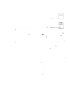
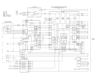
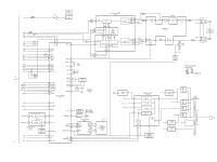
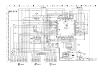
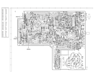
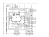
MDS-JE320 6-2. CIRCUIT BOARDS LOCATION SW board DISPLAY board BD board EJECT SW board CONTROL (SW) board - 25 - MAIN board THIS NOTE IS COMMON FOR PRINTED WIRING BOARDS AND SCHEMATIC DIAGRAMS. (In addition to this necessary note is printed in each block.) For schematic diagrams. Note: • All capacitors are in µF unless otherwise noted. pF: µµF 50 WV or less are not indicated except for electrolytics and tantalums. • All resistors are in Ω and 1/4 W or less unless otherwise specified. • % : indicates tolerance. • ¢ : internal component. • 2 : nonflammable resistor. • 1 : fusible resistor. • C : panel designation. Note: The components identified by mark ! or dotted line with mark ! are critical for safety. Replace only with part number specified. Note: Les composants identifiés par une marque ! sont critiques pour la sécurité. Ne les remplacer que par une pièce portant le numéro spécifié. • Waveform • BD SECTION 1 IC101 1,2 I, J (PLAY mode) • MAIN SECTION 1 IC316 @¶ (XOUT) 0.46Vp-p 2 IC101 4 A (PLAY mode) 11.998MHz 3.2Vp-p 2 IC316 @¢ (XOUT-T) 0.1Vp-p 32.77kHz 2.6Vp-p 3 IC101 8,9 E, F (PLAY mode) 3 IC307 0 (LRCK1), @• (LRCK2) • U : B+ Line. • V : B- Line. • H : adjustment for repair. • Voltages and waveforms are dc with respect to ground under no-signal (detuned) conditions. No mark : FM ( ) : PLAY < > : REC • Voltages are taken with a VOM (Input impedance 10 MΩ). Voltage variations may be noted due to normal production tolerances. • Waveforms are taken with a oscilloscope. • Circled numbers refer to waveforms. • Signal path. E :PB q :REC r :REC(DIGITAL IN) a :REC(DIGITAL OUT) 0.06Vp-p 44.1kHz 3.3Vp-p 4 IC121 !§ OSCI 4 IC307 !¡ (BCK1), @§ (BCK2) 22.581MHz 3.1Vp-p 2.822MHz 5.2Vp-p 5 IC121 @∞ LRCK 5 IC307 !∞ (MCK1), @™ (256CK) 44.1KHz 3.2Vp-p 11.29MHz 5.6Vp-p For printed wiring boards. Note: • X : parts extracted from the component side. • ® : Through hole. • ¢ : internal component. • b : Pattern from the side which enables seeing. • p : parts mounted on the conductor side. 6 IC121 @§ XBCK 6 IC307 @∞ (512FS) 2.822KHz 3.8Vp-p 22.581MHz 3.4Vp-p 7 IC121 @¶ FS256 7 IC307 #∞ (XOUT) 11.29MHz 3.8Vp-p 22.58MHz 5Vp-p 8 IC121 (º FS4 176.4KHz • PANEL SECTION 1 IC701 %ª (OSC1) 3.2Vp-p 2.4MHz 3.9Vp-p - 26 -
-
 1
1 -
2
-
3
-
4
-
5
-
6
-
7
-
8
-
9
-
10
-
11
-
12
-
13
-
14
-
15
-
16
-
 17
17 -
 18
18 -
 19
19 -
 20
20 -
 21
21 -
 22
22 -
 23
23 -
 24
24 -
 25
25 -
 26
26 -
 27
27 -
28
-
29
-
30
-
31
-
32
-
33
-
34
-
35
-
36
-
37
-
38
-
39
-
40
-
41
-
42
-
43
-
44
-
45
-
46
-
47
-
48
-
49
-
50
-
51
-
52
-
53
-
54
-
55
-
56
 |
 |
