Sony MDSJE320 Service Manual - Page 38
Ic Pin Functions
 |
UPC - 027242541344
View all Sony MDSJE320 manuals
Add to My Manuals
Save this manual to your list of manuals |
Page 38 highlights
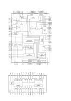
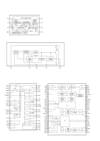
6-15. IC PIN FUNCTIONS • IC101 RF Amplifier (CXA2523R) Pin No. Pin Name I/O 1 I I 2 J I 3 VC O 4 to 9 A to F I 10 PD I 11 APC O 12 APCREF I 13 GND - 14 TEMPI I 15 TEMPR O 16 SWDT I 17 SCLK I 18 XLAT I 19 XSTBY I 20 F0CNT I 21 VREF O 22 EQADJ I/O 23 3TADJ I/O 24 Vcc - 25 WBLADJ I/O 26 TE O 27 CSLED - 28 SE O 29 ADFM O 30 ADIN I 31 ADAGC - 32 ADFG O 33 AUX O 34 FE O 35 ABCD O 36 BOTM O 37 PEAK O 38 RF O 39 RFAGC - 40 AGCI I 41 COMPO O 42 COMPP I 43 ADDC I/O 44 OPO O 45 OPN I 46 RFO O 47 MORFI I 48 MORFO O Function I-V converted RF signal I input I-V converted RF signal J input Middle point voltage (+1.5V) generation output Signal input from the optical pick-up detector Light amount monitor input Laser APC output Reference voltage input for setting laser power Ground Temperature sensor connection Reference voltage output for the temperature sensor Serial data input from the CXD2650R or CXD2652AR Serial clock input from the CXD2650R or CXD2652AR Latch signal input from the CXD2650R or CXD2652AR "L": Latch Stand by signal input "L": Stand by Center frequency control voltage input of BPF22, BPF3T, EQ from the CXD2650R or CXD2652AR Reference voltage output (Not used) Center frequency setting pin for the internal circuit EQ Center frequency setting pin for the internal circuit BPF3T +3V power supply Center frequency setting pin for the internal circuit BPF22 Tracking error signal output to the CXD2650R or CXD2652AR External capacitor connection pin for the sled error signal LPF Sled error signal output to the CXD2650R or CXD2652AR FM signal output of ADIP ADIP signal comparator input ADFM is connected with AC coupling External capacitor connection pin for AGC of ADIP ADIP duplex signal output to the CXD2650R or CXD2652AR I3 signal/temperature signal output to the CXD2650R or CXD2652AR (Switching with a serial command) Focus error signal output to the CXD2650R or CXD2652AR Light amount signal output to the CXD2650R or CXD2652AR RF/ABCD bottom hold signal output to the CXD2650R or CXD2652AR RF/ABCD peak hold signal output to the CXD2650R or CXD2652AR RF equalizer output to the CXD2650R or CXD2652AR External capacitor connection pin for the RF AGC circuit Input to the RF AGC circuit The RF amplifier output is input with AC coupling User comparator output (Not used) User comparator input (Fixed at "L") External capacitor pin for cutting the low band of the ADIP amplifier User operation amplifier output (Not used) User operation amplifier inversion input (Fixed at "L") RF amplifier output Groove RF signal is input with AC coupling Groove RF signal output • Abbreviation APC: Auto Power Control AGC: Auto Gain Control - 54 -
-
 1
1 -
2
-
3
-
4
-
5
-
6
-
7
-
8
-
9
-
10
-
11
-
12
-
13
-
14
-
15
-
16
-
17
-
18
-
19
-
20
-
21
-
22
-
23
-
24
-
25
-
26
-
27
-
28
-
29
-
30
-
31
-
32
-
 33
33 -
 34
34 -
 35
35 -
 36
36 -
 37
37 -
 38
38 -
 39
39 -
 40
40 -
 41
41 -
 42
42 -
 43
43 -
44
-
45
-
46
-
47
-
48
-
49
-
50
-
51
-
52
-
53
-
54
-
55
-
56
 |
 |
