Sony MDSJE320 Service Manual - Page 39
Shock-proof Memory Controller, ATRAC Encoder/Decoder, 2M Bit DRAM CXD2650R or CXD2652AR
 |
UPC - 027242541344
View all Sony MDSJE320 manuals
Add to My Manuals
Save this manual to your list of manuals |
Page 39 highlights
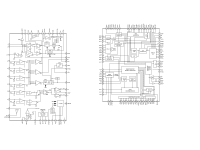
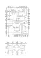
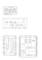
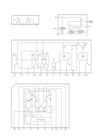
• IC121 Digital Signal Processor, Digital Servo Signal Processor, EFM/ACIRC Encoder/Decoder, Shock-proof Memory Controller, ATRAC Encoder/Decoder, 2M Bit DRAM (CXD2650R or CXD2652AR) Pin No. Pin Name I/O Function 1 MNT0 (FOK) 2 MNT1 (SHCK) FOK signal output to the system control O "H" is output when focus is on O Track jump detection signal output to the system control 3 MNT2 (XBUSY) O Monitor 2 output to the system control 4 MNT3 (SLOC) O Monitor 3 output to the system control 5 SWDT I Writing data signal input from the system control 6 SCLK 7 XLAT I (S) Serial clock signal input from the system control I (S) Serial latch signal input from the system control 8 SRDT O (3) Reading data signal output to the system control 9 SENS O (3) Internal status (SENSE) output to the system control 10 XRST 11 SQSY I (S) Reset signal input from the system control "L": Reset Subcode Q sync (SCOR) output to the system control O "L" is output every 13.3 msec. Almost all, "H" is output 12 DQSY Digital In U-bit CD format subcode Q sync (SCOR) output to the system control O "L" is output every 13.3 msec Almost all, "H" is output 13 RECP 14 XINT I Laser power switching input from the system control "H": Recording, "L": Playback O Interrupt status output to the system control 15 TX I Recording data output enable input from the system control 16 OSCI I System clock input (512Fs=22.5792 MHz) 17 OSCO 18 XTSL O System clock output (512Fs=22.5792 MHz) (Not used) I System clock frequency setting "L": 45.1584 MHz, "H": 22.5792 MHz (Fixed at "H") 19 DVDD - +3V power supply (Digital) 20 DVSS - Ground (Digital) 21 DIN I Digital audio input (Optical input) 22 DOUT O Digital audio output (Optical output) 23 ADDT I Data input from the A/D converter 24 DADT O Data output to the D/A converter 25 LRCK O LR clock output for the A/D and D/A converter (44.1 kHz) 26 XBCK 27 FS256 O Bit clock output to the A/D and D/A converter (2.8224 MHz) O 11.2896 MHz clock output (Not used) 28 DVDD - +3V power supply (Digital) 29 to 32 A03 to A00 O 33 A10 34 to 38 A04 to A08 O O DRAM address output (Used : CXD2652AR, Not used : CXD2650R) 39 A11 O 40 DVSS - Ground (Digital) 41 XOE O Output enable output for DRAM (Used : CXD2652AR, Not used : CXD2650R) 42 XCAS 43 A09 O CAS signal output for DRAM (Used : CXD2652AR, Not used : CXD2650R) O Address output for DRAM (Used : CXD2652AR, Not used : CXD2650R) 44 XRAS O RAS signal output for DRAM (Used : CXD2652AR, Not used : CXD2650R) 45 XWE O Write enable signal output for DRAM (Used : CXD2652AR, Not used : CXD2650R) * I (S) stands for Schmidt input, I (A) for analog input, O (3) for 3-state output, and O (A) for analog output in the column I/O - 55 -
-
 1
1 -
2
-
3
-
4
-
5
-
6
-
7
-
8
-
9
-
10
-
11
-
12
-
13
-
14
-
15
-
16
-
17
-
18
-
19
-
20
-
21
-
22
-
23
-
24
-
25
-
26
-
27
-
28
-
29
-
30
-
31
-
32
-
33
-
 34
34 -
 35
35 -
 36
36 -
 37
37 -
 38
38 -
 39
39 -
 40
40 -
 41
41 -
 42
42 -
 43
43 -
 44
44 -
45
-
46
-
47
-
48
-
49
-
50
-
51
-
52
-
53
-
54
-
55
-
56
 |
 |
