Sony MDSJE320 Service Manual - Page 40
Function, Pin No., Pin Name
 |
UPC - 027242541344
View all Sony MDSJE320 manuals
Add to My Manuals
Save this manual to your list of manuals |
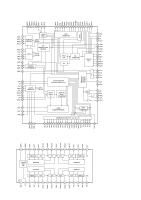
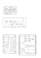
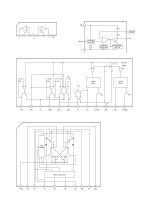
Page 40 highlights
Pin No. 46 47 48, 49 50 51 52 53 54 55 56 Pin Name D1 D0 D2, D3 MVCI ASYO ASYI AVDD BIAS RFI AVSS 57 PDO 58 PCO 59 FILI 60 FILO 61 CLTV 62 PEAK 63 BOTM 64 ABCD 65 FE 66 AUX1 67 VC 68 ADIO 69 AVDD 70 ADRT 71 ADRB 72 AVSS 73 SE 74 TE 75 AUX2 76 DCHG 77 APC 78 ADFG 79 F0CNT 80 XLRF 81 CKRF 82 DTRF 83 APCREF 84 LDDR 85 TRDR I/O Function I/O I/O Data input/output for DRAM (Used : CXD2652AR, Not used : CXD2650R) I/O I (S) Clock input from an external VCO (Fixed at "L") O Playback EFM duplex signal output I (A) Playback EFM comparator slice level input - +3V power supply (Analog) I (A) Playback EFM comparator bias current input I (A) Playback EFM RF signal input - Ground (Analog) Phase comparison output for the clock playback analog PLL of the playback EFM O (3) (Not used) O (3) Phase comparison output for the recording/playback EFM master PLL I (A) Filter input for the recording/playback EFM master PLL O (A) Filter output for the recording/playback EFM master PLL I (A) Internal VCO control voltage input for the recording/playback EFM master PLL I (A) Light amount signal peak hold input from the CXA2523R I (A) Light amount signal bottom hold input from the CXA2523R I (A) Light amount signal input from the CXA2523R I (A) Focus error signal input from the CXA2523R I (A) Auxiliary A/D input I (A) Middle point voltage (+1.5V) input from the CXA2523R O (A) Monitor output of the A/D converter input signal (Not used) - +3V power supply (Analog) I (A) A/D converter operational range upper limit voltage input (Fixed at "H") I (A) A/D converter operational range lower limit voltage input (Fixed at "L") - Ground (Analog) I (A) Sled error signal input from the CXA2523R I (A) Tracking error signal input from the CXA2523R I (A) Auxiliary A/D input (Fixed at "L") I (A) Connected to +3V power supply I (A) Error signal input for the laser digital APC (Fixed at "L") I (S) ADIP duplex FM signal input from the CXA2523R (22.05 ± 1 kHz) O Filter f0 control output to the CXA2523R O Control latch output to the CXA2523R O Control clock output to the CXA2523R O Control data output to the CXA2523R O Reference PWM output for the laser APC O PWM output for the laser digital APC (Not used) O Tracking servo drive PWM output (-) • Abbreviation EFM: Eight to Fourteen Modulation PLL : Phase Locked Loop VCO: Voltage Controlled Oscillator - 56 -
-
 1
1 -
2
-
3
-
4
-
5
-
6
-
7
-
8
-
9
-
10
-
11
-
12
-
13
-
14
-
15
-
16
-
17
-
18
-
19
-
20
-
21
-
22
-
23
-
24
-
25
-
26
-
27
-
28
-
29
-
30
-
31
-
32
-
33
-
34
-
 35
35 -
 36
36 -
 37
37 -
 38
38 -
 39
39 -
 40
40 -
 41
41 -
 42
42 -
 43
43 -
 44
44 -
 45
45 -
46
-
47
-
48
-
49
-
50
-
51
-
52
-
53
-
54
-
55
-
56
 |
 |
