Sony PRS-505/SC Service Manual - Page 34
Main Board, Ic201, R5c807, Memory Stick Duo/sd Memory Card Controller
 |
View all Sony PRS-505/SC manuals
Add to My Manuals
Save this manual to your list of manuals |
Page 34 highlights
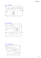
PRS-505 • IC Pin Function Description MAIN BOARD IC201 R5C807 (MEMORY STICK DUO/SD MEMORY CARD CONTROLLER) Pin No. Pin Name I/O Description 1 VCCEN O +3.3V power supply control signal output terminal Not used 2 GPIO I/O Not used 3 LED O Not used 4 HWSPND I Hardware suspend mode select signal input from the main CPU "L": hardware suspend mode 5 RWMODE I Read-write timing mode select signal input terminal "H": maximum cycle time Fixed at "H" in this set 6 WAMODE I WAIT/DTACK mode select signal input terminal "L": DTACK mode, "H": WAIT mode Fixed at "L" in this set 7 LTLEN I Little/big endian select signal input terminal "L": little endian mode, "H": big endian mode Fixed at "L" in this set 8 TEST I Test mode terminal Normally fixed at "L" 9 CKIN I Host colck signal input from the main CPU 10 GND - Ground terminal 11 RST I Reset signal input terminal "L": reset 12 VCC_ROUT - Power supply terminal (+1.8V) 13 VCC_RIN - Power supply terminal (+1.8V) 14 REGEN I Internal regulator control signal input terminal "L": regulator on Fixed at "H" in this set 15 INT O Interrupt request signal output to the main CPU 16 WAIT/DTACK O Data acknowledge signal output terminal Not used 17 WR I Write enable signal input from the main CPU 18 RD I Read enable signal input from the main CPU 19, 20 EB0, EB1 I Byte enable signal input terminal Not used 21 VCC_HOST - Power supply terminal (+3.3V) 22 CS I Chip select signal input from the address decoder 23 to 30 D15 to D8 I/O Two-way data bus with the USB controller, main CPU, SD-RAM and NOR flash memory 31 to 33 D7 to D5 I/O Two-way data bus with the USB controller, main CPU, NAND flash memory, SD-RAM and NOR flash memory 34 GND - Ground terminal 35 to 39 D0 to D4 I/O Two-way data bus with the USB controller, main CPU, NAND flash memory, SD-RAM and NOR flash memory 40 BS I Bus cycle start signal input terminal Not used 41 A22 I Address signal input terminal Not used 42 VCC_ROUT - Power supply terminal (+1.8V) 43 to 47 A21 to A17 I Address signal input terminal Not used 48 VCC_HOST - Power supply terminal (+3.3V) 49 A16 I Address signal input terminal Not used 50 to 64 A15 to A1 I Address signal input from the main CPU 65 A0 I Address signal input terminal Not used 66 GND - Ground terminal 67 SDCD I SD memory card detect signal input from the SD memory card slot "L": SD memory card slot in 68 SDDAT3 I/O Two-way 4-bits data bus with the SD memory card slot 69 MDIO11 I/O Not used 70 MSDAT0 I/O Two-way data bus with the memory stick duo slot 71 MDIO12 I/O Not used 72 MSDAT1 I/O Two-way data bus with the memory stick duo slot 73 VCC_3V - Power supply terminal (+3.3V) 74 MDIO13 I/O Not used 75 MSDAT2 I/O Two-way data bus with the memory stick duo slot 76 MDIO14 I/O Not used 77 MSDAT3 I/O Two-way data bus with the memory stick duo slot 78 to 84 MDIO15, MDIO19 to MDIO24 I/O Not used 85 SDWP I SD memory card write protect switch signal input from the SD memory card slot 86 VCC_ROUT - Power supply terminal (+1.8V) 87 MSCLK O Serial clock signal output to the memory stick duo slot 88 MDIO17 I/O Not used 89 SDCLK O Serial clock signal output to the SD memory card slot 34
-
 1
1 -
2
-
3
-
4
-
5
-
6
-
7
-
8
-
9
-
10
-
11
-
12
-
13
-
14
-
15
-
16
-
17
-
18
-
19
-
20
-
21
-
22
-
23
-
24
-
25
-
26
-
27
-
28
-
 29
29 -
 30
30 -
 31
31 -
 32
32 -
 33
33 -
 34
34 -
 35
35 -
 36
36 -
 37
37 -
 38
38 -
 39
39 -
40
-
41
-
42
-
43
-
44
-
45
-
46
-
47
-
48
-
49
-
50
-
51
-
52
-
53
-
54
-
55
-
56
-
57
-
58
-
59
-
60
-
61
-
62
-
63
-
64
-
65
-
66
-
67
-
68
-
69
-
70
-
71
-
72
-
73
-
74
 |
 |
